Introduction
Signal integrity represents a critical aspect of modern PCB design, particularly as digital signal speeds continue to rise in applications such as telecommunications, computing, and consumer electronics. In high-speed circuits, maintaining the quality of digital signals from source to receiver prevents data errors, system failures, and performance degradation. PCB designers must address multiple factors during the circuit design phase to ensure signals propagate with minimal distortion. These considerations include material properties, layout geometry, and layer stackup, all of which influence impedance matching and loss characteristics. By prioritizing signal integrity early, engineers can achieve reliable operation at data rates exceeding several gigabits per second. This article explores essential PCB considerations for signal integrity, providing structured guidance for electric engineers.
What Is Signal Integrity and Why It Matters in PCB Design
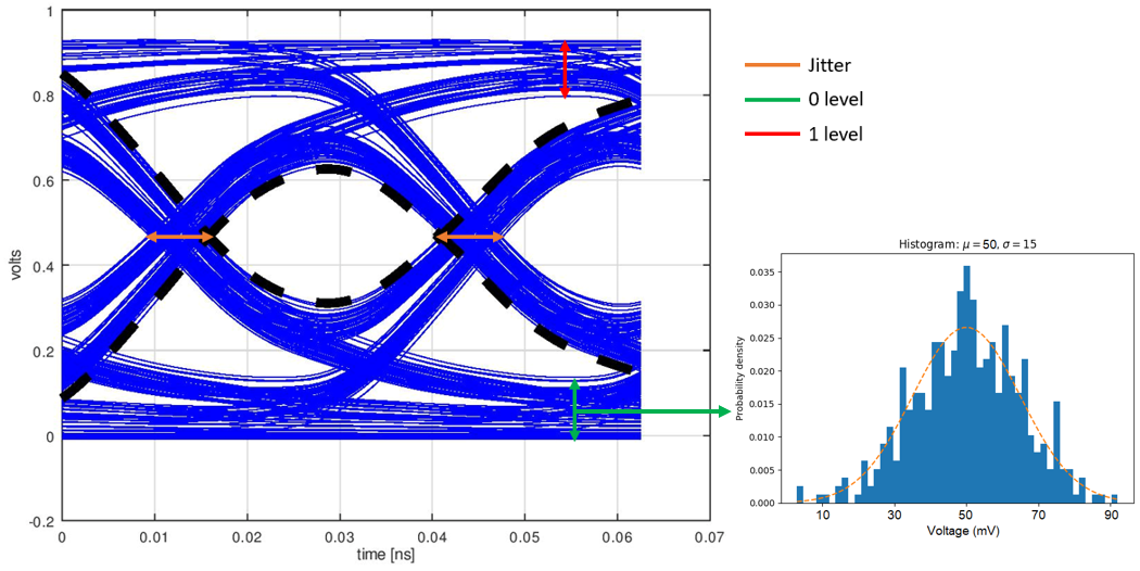
Signal integrity refers to the preservation of electrical signal quality throughout its transmission path on a PCB. For digital signals, this involves minimizing reflections, crosstalk, attenuation, and timing skew that can corrupt data. As edge rates sharpen and frequencies increase, even minor discontinuities become significant, leading to issues like overshoot, ringing, or eye closure in eye diagrams. In PCB design, poor signal integrity manifests as bit errors, reduced margins, or complete system instability, especially in multi-gigabit interfaces.
The relevance intensifies with industry trends toward higher data throughput. Electric engineers face challenges in balancing cost, manufacturability, and performance while adhering to tight timing budgets. Effective signal integrity practices directly impact product reliability and compliance with performance specifications. Neglecting these during circuit design often requires costly respins, underscoring the need for proactive measures from the schematic stage onward.
Fundamental Principles Affecting Signal Integrity on PCBs
Transmission line theory forms the foundation of signal integrity analysis in PCBs. Every trace acts as a transmission line with characteristic impedance determined by geometry and dielectric properties. Mismatches cause reflections, quantified by the reflection coefficient, which degrade signal waveforms. For digital signals, rise times shorter than the propagation delay exacerbate these effects, turning benign layouts into problematic ones.
Crosstalk arises from capacitive and inductive coupling between adjacent traces, coupling noise from aggressor to victim lines. Attenuation stems from conductor and dielectric losses, increasing with frequency due to skin effect and higher dissipation factors. Timing effects, such as skew between differential pairs, further complicate synchronization. Understanding these mechanisms guides PCB choices to control impedance, reduce losses, and isolate signals effectively.
Key PCB Design Considerations for Signal Integrity
Laminate Selection
Laminate selection profoundly impacts signal integrity, especially for high-speed digital signals. The dielectric constant (Dk) influences impedance and propagation velocity, while the dissipation factor (Df) dictates signal loss at high frequencies. Standard FR-4 laminates suffice for lower speeds but exhibit higher Df, leading to excessive attenuation beyond 1 GHz. High-speed laminates with lower Dk and Df values preserve signal amplitude and minimize group delay variations across frequencies.
Engineers must evaluate laminate properties against frequency requirements during circuit design. Thermal stability and CTE matching also prevent warpage that could alter trace dimensions post-fabrication. IPC-4101 provides specifications for base materials, ensuring consistency in laminate performance for multilayer boards. Selecting appropriate high-speed laminates optimizes overall PCB signal integrity without compromising mechanical reliability.
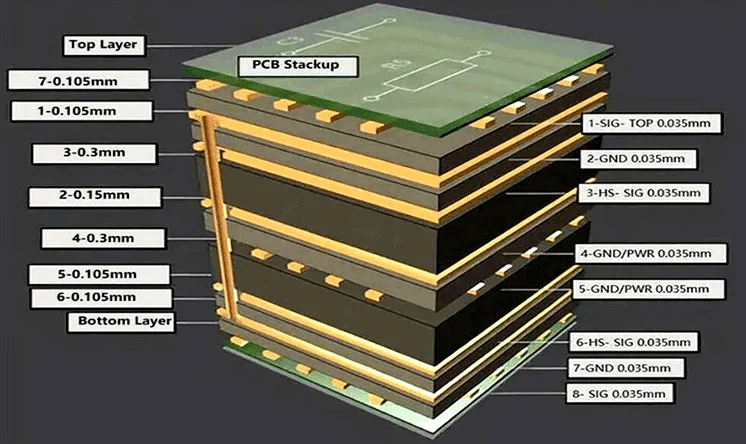
Stackup Design
A well-planned stackup is essential for signal integrity, providing reference planes for return currents and shielding against crosstalk. Symmetric stackups with core and prepreg layers maintain dimensional stability, reducing impedance variations. Placing high-speed signals adjacent to ground or power planes minimizes loop inductance and radiation. Core thickness controls differential pair spacing, directly affecting common-mode impedance.
Power and ground plane pairing forms stripline or microstrip structures, each with trade-offs in loss and manufacturability. Asymmetric stackups risk via stub resonances, so designers prioritize plane proximity for critical nets. Simulations confirm stackup efficacy before layout commitment. This structured approach aligns with IPC-2221 guidelines for multilayer board design.
Related Reading: Signal Integrity for Hobbyists: Simple Tips for Better 8 Layer PCB Designs
Trace Geometry and Routing
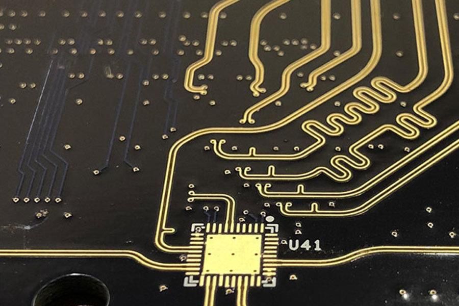
Trace width, spacing, and length profoundly influence impedance control and crosstalk. Wider traces lower impedance but increase coupling if spacing is inadequate; microstrip configurations demand tighter tolerances than striplines. Length matching for differential pairs ensures balanced propagation delays, critical for clock-to-data relationships. Routing avoids right-angle bends, which introduce reflections, favoring 45-degree or curved transitions.
Serpentine routing equalizes lengths while minimizing area, but excessive meandering amplifies losses. Reference plane splits require stitching vias to maintain continuous return paths. Engineers calculate geometries using field solvers during design to hit 50-ohm single-ended or 100-ohm differential targets. These practices form the backbone of robust signal integrity.
Via Design and Transitions
Vias introduce discontinuities, acting as stubs that reflect high-frequency energy. Through-hole vias in multilayer boards create long stubs unless back-drilled to remove unused portions. Blind or buried vias reduce stub length, preserving integrity for signals above 5 GHz. Via capacitance and inductance depend on pad size, anti-pad diameter, and plating thickness.
Optimized via farms for transitions distribute current evenly, mitigating resonance. Ground vias around signal vias shield against crosstalk. During circuit design, minimizing via count per net or using filled vias enhances performance. These considerations prevent common pitfalls in high-density interconnects.
Related Reading: Blind Via Placement Strategies for Optimal Signal Integrity
Best Practices for Signal Integrity in PCB Circuit Design
Implement controlled impedance from the outset by specifying tolerances in fabrication notes, typically 10% for high-speed nets. Use orthogonal routing layers to decouple signals orthogonally, reducing broadside coupling. Incorporate decoupling capacitors near ICs to stabilize power delivery, tying into signal integrity via simultaneous switching noise mitigation.
Pre-layout planning with stackup generators ensures feasibility. Post-layout verification through time-domain reflectometry (TDR) models confirms integrity. Adhering to IPC-2141 for embedded passives and impedance control further refines designs. Collaboration between design and fabrication teams resolves manufacturability issues early.
Troubleshooting Common Signal Integrity Issues
Engineers often encounter eye closure from excessive loss, traced to high-Df laminates or rough copper. Crosstalk spikes indicate inadequate spacing; remedies include guard traces or shielding. Reflections pinpoint impedance mismatches at vias or connectors. Systematic debugging starts with scope captures, followed by modeling adjustments.
Warpage from CTE mismatch distorts traces, addressed via symmetric stackups. Thermal effects exacerbate losses, necessitating low-loss high-speed laminates. Case studies reveal that iterative simulation resolves 80% of issues pre-prototype. Proactive design per standards prevents recurrence.
Conclusion
Signal integrity demands meticulous PCB considerations throughout circuit design, from laminate selection to via optimization. High-speed laminates, precise stackups, and controlled routing preserve digital signal quality amid rising frequencies. By applying these principles, electric engineers mitigate risks, enhance reliability, and meet performance goals. Integrating industry standards ensures consistency and manufacturability. Prioritizing these factors yields robust designs ready for production.
FAQs
Q1: What role does laminate selection play in PCB signal integrity?
A1: Laminate selection affects dielectric properties critical for high-speed digital signals. Low Dk and Df in high-speed laminates reduce attenuation and maintain impedance stability. Engineers evaluate these against frequency needs to prevent signal degradation. Proper choice aligns with IPC-4101 specifications for base materials, ensuring reliable performance in multilayer PCBs.
Q2: How does stackup design impact signal integrity on PCBs?
A2: Stackup design influences return paths, crosstalk, and impedance control. Adjacent planes shield signals and minimize inductance. Symmetric configurations prevent warpage-induced variations. For digital signals, this setup supports gigabit speeds without distortion. Following IPC-2221 guidelines optimizes layer pairing for integrity.
Q3: Why is via design crucial for high-speed PCB signal integrity?
A3: Vias create discontinuities that reflect signals if not optimized. Backdrilling or blind vias shorten stubs, preserving waveform fidelity. Proper anti-pad sizing reduces capacitance. In high-speed laminates, this maintains low loss. Engineers prioritize via strategies during circuit design to avoid resonances.
Q4: What are best practices for trace routing in signal integrity?
A4: Controlled width and spacing ensure 50-ohm impedance matching. Length tuning for pairs prevents skew. Avoid splits in reference planes with stitching vias. Orthogonal routing layers decouple signals. These practices, rooted in transmission line principles, uphold digital signal quality across the PCB.
References
IPC-2221B — Generic Standard on Printed Board Design. IPC, 2003
IPC-2141 — Design Standard for Rigid Printed Boards and Rigid Printed Board Assemblies with Embedded Components. IPC, 2020
IPC-4101E — Specification for Base Materials for Rigid and Multilayer Printed Boards. IPC, 2017