Introduction
In the PCB manufacturing process, etching represents a critical step where unwanted copper is selectively removed to form conductive traces and patterns. The quality of these traces directly influences the electrical performance, reliability, and overall functionality of the printed circuit board. Variations in etching parameters can lead to defects such as undercutting, rough sidewalls, or inconsistent widths, compromising PCB trace quality. Engineers must understand these parameters to optimize production yields and meet stringent performance requirements. This article delves into the key etching parameters, their effects on trace quality, and strategies for control. By examining these factors, professionals can enhance design margins and reduce failure risks in high-density interconnects.
What Are Etching Parameters and Why Do They Matter for PCB Trace Quality?
Etching parameters refer to the controllable variables in the chemical etching stage of PCB fabrication, primarily including etching temperature, etchant concentration, and etching time. These factors govern the rate and uniformity of copper dissolution, directly impacting the dimensional accuracy and surface finish of traces. Poor control can result in overetching, where traces become narrower than designed, or underetching, leading to residual copper bridges. In high-frequency applications, such imperfections degrade signal integrity and increase insertion loss. Adhering to standards like IPC-6012 ensures that trace geometries meet qualification criteria for rigid printed boards. Ultimately, mastering these parameters is essential for achieving consistent PCB trace quality across production runs.
The relevance extends to the entire supply chain, as trace defects often manifest as shorts, opens, or impedance mismatches during assembly and testing. Factory insights reveal that parameter drift accounts for a significant portion of yield losses in multilayer boards. Engineers rely on precise etching to maintain conductor spacing and width tolerances, critical for routing density in modern designs. Without optimization, even advanced laminates fail to deliver expected performance.
The Role of Etching Temperature in PCB Trace Quality
Etching temperature profoundly affects the reaction kinetics in the etching bath, accelerating the dissolution of copper as it rises. Higher temperatures increase etch rates exponentially, potentially causing rapid undercutting if not balanced with other parameters. This leads to tapered sidewalls and reduced trace widths, violating dimensional specs in dense patterns. Conversely, low temperatures slow the process, risking incomplete etch and adhesion issues with subsequent layers. Maintaining a stable temperature, typically through circulation systems, ensures uniform etching across the panel. Fluctuations greater than a few degrees can amplify defects in fine-line traces below 100 microns.
The chemical mechanism involves enhanced ion mobility and reaction activation at elevated temperatures, but excessive heat promotes isotropic etching, eroding the copper mask interface. In practice, factories monitor temperature to align with etchant chemistry, such as cupric chloride solutions. This parameter interacts closely with time and concentration, demanding holistic control. IPC-A-600 provides acceptability criteria for etched features, emphasizing smooth sidewalls free of excessive pitting. Engineers should profile temperature ramps to minimize thermal gradients on large panels.
Influence of Etchant Concentration on Etching Uniformity
Etchant concentration determines the availability of reactive species, directly dictating etch rate and selectivity. Dilute solutions etch slowly and uniformly but may leave residues, while concentrated ones attack copper aggressively, leading to overetch and rough edges. Imbalanced concentrations cause preferential etching at trace edges, resulting in hourglass profiles that weaken mechanical integrity. Regular replenishment and titration maintain optimal levels, preventing byproduct buildup that inhibits reaction. Deviations impact fine-pitch designs most severely, where trace quality dictates high-speed signal propagation.
Concentration gradients across the bath exacerbate nonuniformity, especially in spray etching systems. Engineers analyze spent etchant to adjust makeup solutions, ensuring consistent copper loading. This parameter's interplay with temperature amplifies effects; high concentration at low temperature yields controlled etches. Standards like J-STD-001 highlight the need for clean conductor surfaces post-etching to support reliable soldering. Proactive monitoring via inline sensors enhances PCB manufacturing process repeatability.
Etching Time and Its Critical Effects on Trace Dimensions
Etching time controls total material removal, where insufficient duration leaves copper foils intact, creating opens or weak points. Prolonged exposure induces lateral etching, narrowing traces and increasing resistance. Precise timing, synchronized with conveyor speed in inline systems, achieves target breakthrough without excess undercut. Factors like panel loading and pattern density necessitate dynamic adjustments to avoid batch variations. Over time, trace quality suffers from cumulative errors, manifesting as yield drops in electrical testing.
The etch endpoint detection, often via optical or conductivity probes, signals completion to halt undercutting. In panel processing, inner layers demand shorter times due to smaller feature sizes. Engineers calibrate time based on copper weight, ensuring compliance with design rules. This parameter's sensitivity underscores the need for automated controls in volume production.
Mechanisms of Etching Defects and Trace Quality Degradation
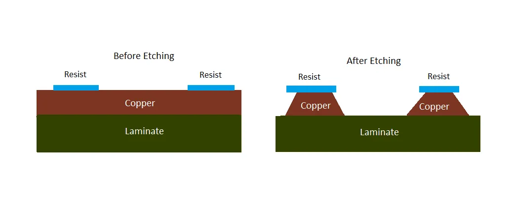
Etching proceeds isotropically in most chemistries, dissolving copper equally in all directions and inherently causing undercut beneath the resist. Parameters modulate this by influencing diffusion-limited rates at the etch front. High etching temperature or concentration accelerates bulk etching but starves edges of fresh etchant, leading to faceting or nodules. Etching time compounds these if not endpoint-controlled, eroding trace integrity. Agitation mitigates stagnation, promoting even reactant delivery for superior sidewall profiles.
Resist adhesion failures under aggressive conditions expose copper prematurely, amplifying defects. Post-etch residues from depleted etchant compromise cleanliness, affecting plating or solder mask application. Understanding these interactions allows predictive modeling of trace tolerances. Factories implement statistical process control to track parameter excursions against quality metrics.
Best Practices for Optimizing Etching Parameters
Establish baseline profiles through design of experiments, varying one parameter while holding others constant to map etch rates. Implement closed-loop controls integrating temperature, concentration, and time feedback for real-time adjustments. Regular bath maintenance, including filtration and regeneration, sustains performance. Use standardized test coupons to verify trace quality post-etch, aligning with IPC criteria. Train operators on anomaly recognition, such as uneven panel etching signaling pump failures.
For high-reliability boards, opt for conveyorized spray etching over immersion for better uniformity. Simulate parameter sets virtually to predict outcomes before production. Document deviations and root causes to refine processes iteratively. These practices elevate PCB trace quality, minimizing rework and supporting advanced node capabilities.
Troubleshooting Common Etching-Related Trace Defects
Overetching, evident as narrowed traces, often stems from excessive time or high temperature; shorten exposure or cool the bath incrementally. Undercut minimization requires balanced concentration to avoid edge acceleration. Rough sidewalls signal inadequate agitation; upgrade nozzles or increase flow rates. Residual copper points to low etchant activity; titrate and replenish promptly. Cross-section analysis confirms root causes, guiding corrections.
Panel warpage from uneven etching calls for fixturing and symmetric loading. Electrical test failures post-etch highlight opens from incomplete removal, addressed by endpoint refinement. Systematic logging correlates defects to parameters, fostering continuous improvement.
Conclusion
Etching parameters like temperature, concentration, and time are pivotal in determining PCB trace quality during manufacturing. Precise control prevents defects such as undercutting and rough edges, ensuring reliable electrical performance. By leveraging standard-aligned practices and monitoring tools, engineers achieve consistent results across production scales. Integrating these insights into workflows enhances yield and supports complex designs. Prioritizing parameter optimization remains a cornerstone of robust PCB fabrication.
FAQs
Q1: How does etching temperature affect PCB trace quality?
A1: Etching temperature accelerates copper dissolution rates, influencing sidewall profiles and trace widths. Elevated temperatures risk overetching and undercutting, while low ones cause incomplete removal. Factories stabilize it via heat exchangers to meet tolerances. Consistent control ensures uniform PCB trace quality, vital for signal integrity in high-density boards.
Q2: What role does etchant concentration play in the PCB manufacturing process?
A2: Etchant concentration governs reaction speed and uniformity during etching. High levels promote aggressive etching with potential roughening, low ones lead to residues. Regular analysis maintains balance, preventing trace defects. This parameter directly impacts PCB trace quality by controlling undercut and edge definition.
Q3: How can etching time be optimized for better PCB trace quality?
A3: Etching time must match pattern density and copper thickness to avoid over or underetch. Endpoint detection halts the process precisely, preserving dimensions. Adjustments based on inline monitoring refine outcomes. Proper timing in the PCB manufacturing process yields traces with smooth sidewalls and accurate widths.
Q4: Why are etching parameters critical for high-reliability PCBs?
A4: Etching parameters ensure trace geometries comply with standards, minimizing impedance variations and failures. Interactions between temperature, concentration, and time demand holistic management. Optimized settings reduce defects like pitting or narrowing. Superior PCB trace quality supports demanding applications in aerospace and telecom.
References
- IPC-6012E - Qualification and Performance Specification for Rigid Printed Boards. IPC, 2017
- IPC-A-600K - Acceptability of Printed Boards. IPC, 2020
- J-STD-001H - Requirements for Soldered Electrical and Electronic Assemblies. IPC, 2018