Introduction
Printed Circuit Board (PCB) imaging and inspection are vital processes in electronics manufacturing, ensuring the quality and reliability of every board produced. For electrical engineers, understanding the complexities of PCB inspection is essential to address design flaws, assembly errors, and material issues early in the production cycle. With the increasing demand for miniaturized components and intricate layouts, manufacturers face significant challenges in achieving accurate imaging and consistent inspection results. Issues such as component spacing constraints, material selection impacts, and the integration of automated systems further complicate the process. This article explores the core challenges in PCB imaging, delving into technical hurdles and offering practical insights for overcoming them. By focusing on design considerations, assembly practices, and automated inspection methods, engineers can better navigate these obstacles to ensure high quality output.
What Is PCB Imaging and Why It Matters
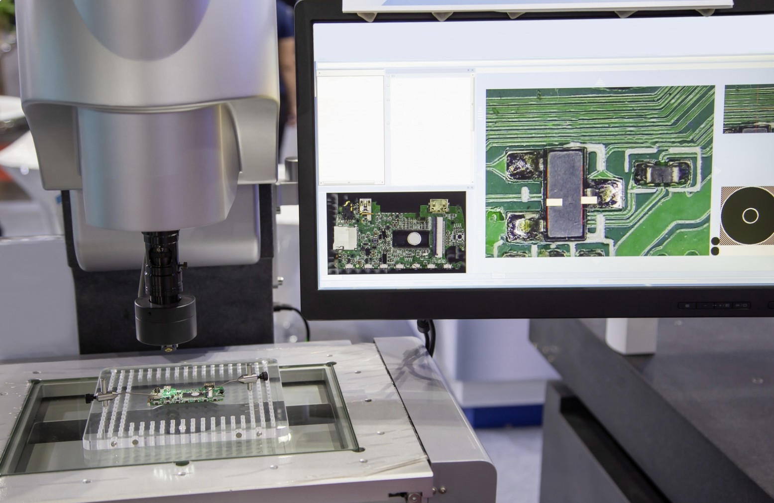
PCB imaging refers to the process of capturing detailed visual or digital representations of a printed circuit board to assess its structure, components, and potential defects. This step is critical during inspection, where the goal is to verify that the board meets design specifications and industry standards. For electrical engineers, PCB imaging matters because it directly influences the functionality and reliability of electronic devices. A single undetected flaw, such as a misaligned component or a microscopic crack, can lead to system failures. With the rise of complex designs and tighter component spacing, imaging accuracy has become more crucial than ever. Moreover, as automated PCB assembly systems gain prominence, imaging serves as the backbone of quality control, enabling real time defect detection and reducing manual errors in high volume production environments.
Related Reading: Selecting the Right PCB Inspection Equipment: A Guide to AOI, X Ray, and Flying Probe Testing
Technical Challenges in PCB Imaging and Inspection
Resolution Limitations with Miniaturized Designs
As electronic devices shrink in size, PCB designs incorporate increasingly smaller components with minimal spacing. This trend poses a significant challenge for imaging systems, which must achieve high resolution to detect minute defects like hairline cracks or solder joint issues. Insufficient resolution can result in missed flaws, particularly in densely packed areas where component spacing is below a millimeter. Engineers often struggle to balance imaging precision with inspection speed, especially in automated setups where throughput is a priority. The challenge intensifies with multilayer boards, where inner layers remain hidden from standard optical methods, necessitating advanced techniques to capture accurate data without compromising efficiency.
Material Selection and Imaging Interference
Material selection plays a critical role in PCB imaging outcomes. Different substrates and coatings can interfere with imaging systems, causing reflections or distortions that obscure defects. For instance, highly reflective surfaces may create glare, while dark or matte finishes can absorb light, reducing image clarity. Additionally, the choice of solder mask materials can affect how imaging systems interpret surface features, sometimes masking underlying issues. Electrical engineers must consider these factors during the design phase to ensure compatibility with inspection tools. Poor material choices can lead to false positives or negatives during automated inspection, increasing the risk of defective boards reaching the assembly stage.
Component Spacing and Shadowing Effects
Tight component spacing, a common requirement in modern PCB design, introduces shadowing effects during imaging. Tall components can block light or obscure adjacent areas, making it difficult to inspect nearby solder joints or traces. This issue is particularly pronounced in automated PCB assembly, where precise placement is critical, yet imaging systems may fail to capture hidden defects. Engineers face the challenge of designing layouts that minimize shadowing while meeting functional requirements. Without proper consideration, inspection accuracy suffers, leading to potential failures in the final product. Addressing this requires a combination of optimized design practices and advanced imaging technologies.
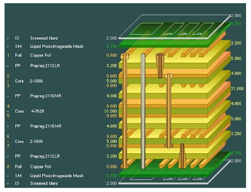
Multilayer Board Complexity
Multilayer PCBs, widely used in high performance applications, add another layer of difficulty to imaging and inspection. Inner layers are inaccessible to standard optical systems, requiring specialized methods to detect internal defects such as delamination or misaligned vias. While these techniques improve visibility, they often increase inspection time and cost, posing a challenge for manufacturers aiming for efficiency in automated processes. Electrical engineers must account for these complexities during design, ensuring that multilayer structures are compatible with available inspection methods to maintain quality without sacrificing production speed.
Limitations of Automated Inspection Systems
Automated inspection systems, while efficient, are not without flaws. These systems rely on predefined algorithms and imaging setups, which may struggle to adapt to unique PCB designs or unexpected defects. For instance, variations in component placement or material properties can lead to misinterpretation of data, resulting in false defect reports. Additionally, automated systems may lack the sensitivity to detect subtle issues that a trained human inspector might notice. Engineers working on PCB assembly must calibrate these systems carefully, ensuring they align with specific design and material parameters to minimize errors during high volume production runs.
Related Reading: How Does Lighting Impact Automated Optical Inspection (AOI) for PCBs?
Practical Solutions for PCB Imaging Challenges
Optimizing Design for Inspection
One of the most effective ways to address imaging challenges is through thoughtful PCB design. Electrical engineers can prioritize layouts that reduce shadowing by strategically placing taller components away from critical inspection areas. Additionally, maintaining adequate component spacing, even in compact designs, allows imaging systems to capture clearer data without obstruction. Adhering to industry standards, such as those outlined in IPC-A-600K, helps ensure that designs are inspection friendly, minimizing the risk of overlooked defects. During the design phase, simulating potential imaging issues can also guide adjustments before production begins.
Material Selection Guidelines
Choosing the right materials is essential for reliable PCB imaging. Engineers should select substrates and solder masks with properties that enhance image clarity, avoiding highly reflective or overly dark finishes. Consulting standards like IPC-6012E for material performance specifications can guide decisions, ensuring compatibility with common inspection tools. Testing material samples under actual imaging conditions before full scale production can reveal potential interferences, allowing for adjustments early in the process. This proactive approach reduces the likelihood of imaging errors during automated inspection.
Advanced Imaging Technologies
Leveraging advanced imaging technologies offers a robust solution to many inspection challenges. Techniques that penetrate multiple layers can uncover internal defects in complex boards, while high resolution cameras improve detection of microscopic flaws in miniaturized designs. Automated systems equipped with adaptive algorithms can better handle variations in PCB layouts, reducing false readings. Electrical engineers should stay informed about emerging imaging tools, integrating them into assembly workflows to enhance accuracy. Combining multiple imaging methods can also provide a comprehensive view, addressing limitations of individual systems.
Calibration and Training for Automated Systems
For automated PCB assembly and inspection, proper calibration of imaging systems is crucial. Engineers must regularly adjust settings to match specific board designs, material properties, and component layouts. Training personnel to interpret automated inspection outputs ensures that subtle defects are not overlooked, complementing machine capabilities with human expertise. Following guidelines from standards such as ISO 9001:2015 for quality management can help establish consistent calibration protocols. Routine maintenance of equipment further prevents drifts in accuracy, supporting reliable inspection across production batches.
Insight: Balancing Speed and Accuracy in Automated Inspection
In high volume PCB manufacturing, striking a balance between inspection speed and accuracy remains a persistent challenge for electrical engineers. Automated systems are designed to maximize throughput, often processing thousands of boards per hour. However, rushing the imaging process can compromise defect detection, especially for intricate designs with tight component spacing. One practical approach is to implement tiered inspection protocols, where critical areas of a PCB undergo detailed scanning while less complex regions are assessed more quickly. This method, aligned with quality control practices in IPC-A-600K, optimizes efficiency without sacrificing reliability. Engineers should also periodically review automated system performance, adjusting parameters to address evolving design complexities and material variations in assembly lines.

Conclusion
PCB imaging and inspection are indispensable for ensuring the quality of printed circuit boards, yet manufacturers face numerous challenges in achieving consistent results. From resolution limitations in miniaturized designs to material interferences and component spacing issues, each obstacle demands careful consideration during design and assembly phases. By optimizing PCB layouts, selecting compatible materials, and leveraging advanced imaging technologies, electrical engineers can mitigate many of these issues. Additionally, fine tuning automated inspection systems and adhering to industry standards enhances reliability in high volume production. Addressing these challenges not only improves manufacturing outcomes but also ensures that electronic devices meet the rigorous demands of modern applications, fostering trust in every board produced.
FAQs
Q1: How does component spacing affect PCB imaging during inspection?
A1: Component spacing significantly impacts PCB imaging by influencing visibility during inspection. Tightly packed components can create shadowing effects, obscuring solder joints or traces from imaging systems. This often leads to missed defects, especially in automated setups. Electrical engineers must design layouts with adequate spacing to ensure clear imaging, balancing compactness with inspection needs as per standards like IPC-A-600K.
Q2: What role does material selection play in automated PCB inspection?
A2: Material selection is crucial for automated PCB inspection as it affects image clarity. Reflective or dark substrates can cause glare or light absorption, leading to distorted imaging data. Choosing materials compatible with inspection tools, guided by standards like IPC-6012E, minimizes errors. Testing materials beforehand ensures they support accurate defect detection in automated systems.
Q3: How can PCB design improve inspection outcomes in assembly?
A3: Thoughtful PCB design enhances inspection outcomes by reducing imaging obstacles in assembly. Strategically placing components to avoid shadowing and maintaining proper spacing allows clearer imaging. Following standards such as IPC-A-600K during design ensures compatibility with inspection methods. Simulating imaging challenges early helps engineers adjust layouts, improving automated inspection accuracy.
Q4: Why is calibration important for automated PCB assembly inspection?
A4: Calibration is vital for automated PCB assembly inspection to ensure system accuracy. Misaligned settings can lead to false defect readings, especially with varied designs or materials. Regular calibration, aligned with ISO 9001:2015 guidelines, matches equipment to specific board parameters. This practice, combined with operator training, maintains reliability across production runs.
References
IPC-A-600K — Acceptability of Printed Boards. IPC, 2020.
IPC-6012E — Qualification and Performance Specification for Rigid Printed Boards. IPC, 2017.
ISO 9001:2015 — Quality Management Systems. ISO, 2015.


