Introduction
In the relentless pursuit of higher performance and miniaturization, modern electronic devices, particularly those in high power, high frequency, and harsh environments, generate significant amounts of heat. Effective thermal management is not merely a design consideration; it is a critical enabler for ensuring system reliability, maintaining operational stability, and extending the lifespan of sensitive electronic components. While conventional FR-4 printed circuit boards (PCBs) struggle to cope with escalating thermal loads, ceramic PCB technology emerges as a superior solution. This article delves into the thermal management secrets of optimizing heat dissipation with ceramic PCBs, highlighting their unique advantages and the specialized design and manufacturing techniques required for high power PCB design.
What is Ceramic PCB Thermal Management and Why it Matters
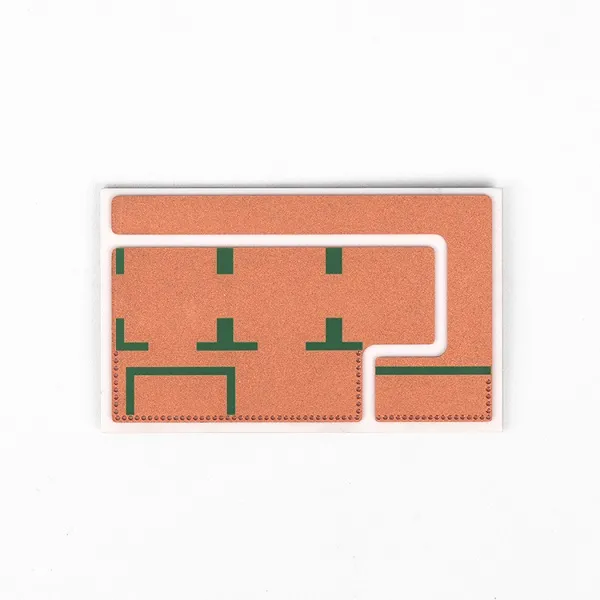
Ceramic PCB thermal management refers to the comprehensive strategy of utilizing ceramic substrates to efficiently extract, spread, and dissipate heat generated by active components within an electronic assembly. Unlike organic laminates, ceramic materials possess intrinsic properties that make them exceptional thermal conductors.
The importance of robust thermal management cannot be overstated in high power and densely packed electronic systems. Without effective ceramic PCB cooling, excessive heat can lead to:
- Reduced Component Lifespan: Elevated temperatures accelerate material degradation, particularly in semiconductors and electrolytic capacitors, leading to premature failure.
- Performance Degradation: Integrated circuits may experience thermal throttling, voltage drift, or outright functional failure when their operating junction temperatures are exceeded.
- Solder Joint Reliability Issues: Differential thermal expansion between components and the PCB can induce mechanical stress on solder joints, causing fatigue and failure over time.
- System Instability: Uncontrolled temperature rises can lead to increased noise, signal integrity issues, and unpredictable circuit behavior.
Therefore, leveraging the inherent thermal advantages of ceramic PCBs is fundamental for achieving the stringent reliability and performance targets of next generation electronics.
Unique Thermal Advantages of Ceramic PCBs
Ceramic materials stand out for their exceptional thermal properties, making them ideal for high power PCB design.
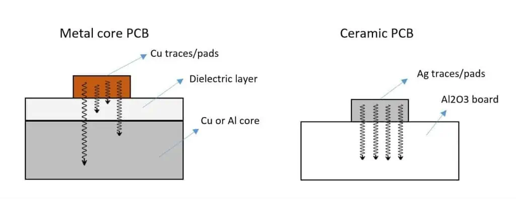
- Superior Thermal Conductivity: This is the most significant advantage. While standard FR-4 has a thermal conductivity of approximately 0.25 W/m·K, ceramic materials offer vastly superior performance. Alumina (Al2O3), the most common ceramic substrate, provides thermal conductivities ranging from 20 to 30 W/m·K. For extremely demanding applications, aluminum nitride (AlN) boasts even higher thermal conductivity, typically between 170 to 220 W/m·K. This enables heat to be drawn away from components and spread rapidly across the substrate.
- Excellent Coefficient of Thermal Expansion (CTE) Match: Ceramic materials exhibit very low CTEs that closely match those of silicon semiconductor chips (silicon's CTE is approximately 2.6 ppm/°C). For instance, alumina has a CTE of around 7 ppm/°C, and aluminum nitride is about 4.7 ppm/°C. This close match minimizes thermal stress at the interface between the semiconductor die and the PCB substrate during temperature cycling, greatly enhancing the reliability of direct die attach (chip on board) and wire bonding applications.
- High Temperature Resistance: Ceramic substrates can withstand significantly higher operating temperatures without degradation compared to organic laminates. Their high melting points and excellent thermal stability make them suitable for extreme thermal environments where FR-4 would fail.
- Electrical Insulation: Despite their excellent thermal conductivity, ceramic materials are superb electrical insulators, ensuring electrical isolation between circuit layers and components while facilitating heat transfer.
Key Strategies for Optimizing Heat Dissipation with Ceramic PCBs
Optimizing heat dissipation with ceramic PCBs involves a combination of material selection, advanced manufacturing techniques, and meticulous design practices.
1. Strategic Material Selection: Alumina vs. Aluminum Nitride
The choice between different ceramic materials depends directly on the thermal demands of the application.
- Alumina (Al2O3) for Moderate to High Power: For applications requiring good thermal performance at a more accessible cost, alumina is an excellent choice. Its thermal conductivity is sufficient for many power modules, LED arrays, and RF applications.
- Aluminum Nitride (AlN) for Extreme Power: When heat generation is exceptionally high, such as in high power laser diodes, IGBT modules, or advanced radar systems, aluminum nitride is the preferred substrate. Its ultra high thermal conductivity provides the most efficient direct path for heat removal.
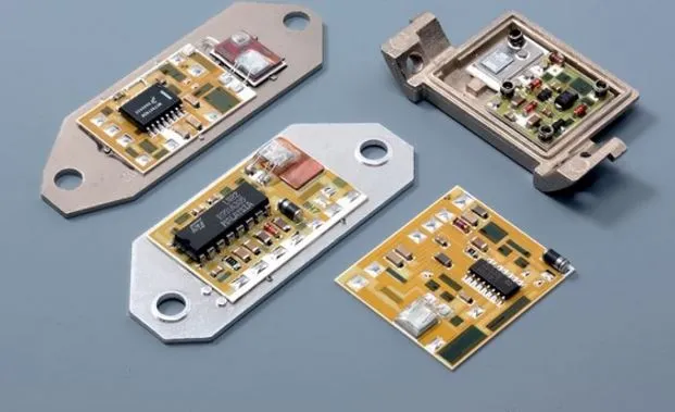
2. Direct Bonded Copper (DBC) and Active Metal Brazing (AMB)
These specialized manufacturing techniques are critical for maximizing thermal transfer from high power components.
- DBC (Direct Bonded Copper): In DBC technology, pure copper foil is directly bonded to a ceramic substrate (typically alumina or aluminum nitride) at high temperatures without an adhesive layer. This creates an extremely strong and highly thermally conductive interface, allowing heat to flow directly from the copper circuit traces into the ceramic base with minimal thermal resistance.
- AMB (Active Metal Brazing): Similar to DBC, AMB also creates a strong metallurgical bond between copper and ceramic, often used for even more demanding power cycling applications.
- Impact: Both DBC and AMB are essential for high power PCB design on ceramic, providing a robust and efficient thermal pathway for ceramic PCB cooling.
3. Thick Copper Metallization
Unlike standard PCBs, ceramic PCBs often utilize much thicker copper layers (e.g., 100 µm to 600 µm or more).
- Enhanced Lateral Heat Spreading: Thicker copper metallization significantly improves the lateral heat spreading capability on the ceramic surface before the heat is conducted downwards. This helps to distribute heat more evenly and avoid localized hot spots.
- Higher Current Carrying Capacity: Heavy copper is also beneficial for high power PCB design by allowing higher current densities with minimal resistive losses.
- IPC-2152: This standard, Standard for Determining Current-carrying Capacity in Printed Board Design, provides guidelines for copper trace sizing, which can be adapted for ceramic PCBs.
4. Thermal Via Design
While the ceramic itself is an excellent thermal conductor, thermal via design plays a role in specific scenarios.
- Connecting Multiple Copper Layers: In multi layer ceramic constructions (less common than single layer, but possible), thermal vias can connect heat spreading copper planes through the ceramic, ensuring efficient vertical heat flow.
- Localizing Heat Transfer: For components without exposed thermal pads that are mounted on top of a copper trace, strategically placed thermal vias within the copper pad can help channel heat more directly into the underlying ceramic.
- Ground Connections: Thermal vias often double as ground vias, providing low inductance electrical connections to the ceramic's metallized backside, which can serve as a large ground plane and heat sink.
5. Component Placement Optimization
Strategic component placement is always critical, but even more so for maximizing ceramic PCB thermal management.
- Proximity to Heat Sink: High power, heat generating components should be placed directly over the most thermally conductive areas of the ceramic substrate.
- Even Distribution: Distribute heat sources across the ceramic substrate to prevent localized thermal saturation and ensure uniform heat spreading.
- Direct Contact: Components with exposed thermal pads should be soldered to matching pads on the ceramic PCB, ensuring a direct and low resistance thermal path.
6. Integration with External Cooling Solutions
Even with the superior intrinsic thermal performance of ceramic PCBs, some extremely high power applications may still require external cooling.
- Heat Sinks: The ceramic substrate can act as an excellent interface for attaching external heat sinks, providing a very low thermal resistance path from the component to the heat sink.
- Liquid Cooling: For the most demanding applications, the ceramic PCB can be integrated with microchannel liquid cooling systems, leveraging its high thermal conductivity to transfer heat rapidly to a circulating coolant.
Manufacturing Considerations for Ceramic PCB Cooling
The fabrication of ceramic PCBs, especially those optimized for thermal performance, involves specialized manufacturing processes.
- Precision Etching: Achieving fine line features on thick copper layers bonded to ceramic requires precise etching controls.
- High Temperature Processing: DBC and AMB processes involve very high temperatures, which ceramic substrates can withstand, but require specialized equipment and atmosphere control.
- Laser Drilling: For microvias or complex geometries, laser drilling is often used due to the hardness of ceramic materials.
- Quality Control: Stringent quality control, including thermal cycling tests (e.g., JEDEC JESD22-A104E, Temperature Cycling) and Dielectric Withstand Voltage (DWV) testing, is crucial to ensure the long term reliability and electrical integrity of ceramic PCBs for high power applications.
Thermal Analysis and Verification
Accurate thermal analysis and verification are indispensable for validating ceramic PCB thermal management designs.
- Computational Fluid Dynamics (CFD) and Finite Element Analysis (FEA): Advanced simulation tools use CFD and FEA to model heat transfer within the ceramic PCB and its components. These analyses predict temperature distributions, identify potential hot spots, and optimize material selection and layout before physical prototyping.
- Thermal Imaging and Testing: Infrared (IR) cameras provide real time thermal maps of operational ceramic PCBs, allowing engineers to verify simulation results, assess the effectiveness of ceramic PCB cooling strategies, and fine tune the design.
- Reliability Testing: Beyond basic functional tests, accelerated life testing, and power cycling are performed to evaluate the long term durability and thermal stability of the ceramic PCB and its components under simulated operational stresses.
Conclusion
Ceramic PCBs are not just an alternative to FR-4; they are a fundamental solution for effective thermal management in modern high power PCB design. By leveraging their intrinsically superior thermal conductivity, excellent CTE match with silicon, and high temperature resistance, designers can achieve unparalleled heat dissipation. Advanced manufacturing techniques like DBC and AMB, combined with meticulous design strategies for material selection, copper metallization, thermal via design, and component placement, unlock the full potential of ceramic PCB cooling. The strategic adoption of ceramic PCBs, supported by rigorous analysis and verification, is a key enabler for the development of highly efficient, reliable, and compact electronic systems that meet the escalating thermal challenges of today's technology.
FAQs
Q1: What are the primary thermal advantages of ceramic PCBs over FR-4 for high power applications?
A1: The primary thermal advantages of ceramic PCBs include significantly higher thermal conductivity (e.g., AlN up to 220 W/m·K vs. FR-4's 0.25 W/m·K), an excellent CTE match with silicon chips, and superior high temperature resistance. These properties ensure efficient heat dissipation and enhanced reliability in high power PCB design.
Q2: How do Direct Bonded Copper (DBC) and Active Metal Brazing (AMB) contribute to ceramic PCB thermal management?
A2: DBC and AMB are crucial for ceramic PCB thermal management as they create an extremely strong and highly thermally conductive metallurgical bond between thick copper and the ceramic substrate. This direct interface minimizes thermal resistance, allowing heat to flow rapidly and efficiently from components into the ceramic base for ceramic PCB cooling.
Q3: Is thermal via design as critical for ceramic PCBs as it is for FR-4 in heat dissipation?
A3: Thermal via design is still important for ceramic PCBs but for different reasons than FR-4. On ceramic, vias are often used to connect heat spreading copper layers or to localize heat transfer from specific component pads into the ceramic base, which itself is already an excellent thermal conductor, thereby optimizing heat dissipation.
Q4: What ceramic materials are best for extreme high power PCB cooling?
A4: For extreme high power PCB cooling, Aluminum Nitride (AlN) ceramic is generally considered the best material. It offers exceptional thermal conductivity, typically ranging from 170 to 220 W/m·K, providing the most efficient heat transfer for the most demanding high power PCB design applications.
References
IPC-2152 — Standard for Determining Current-carrying Capacity in Printed Board Design. IPC, 2009.
IPC-2221A — Generic Standard on Printed Board Design. IPC, 2003.
JEDEC JESD22-A104E — Temperature Cycling. JEDEC, 2019.