What is ENIG and Why Is Its Performance Critical?
Electroless Nickel Immersion Gold (ENIG) is a widely adopted surface finish in the manufacturing of Printed Circuit Boards (PCBs). This finish consists of an initial layer of nickel deposited onto copper pads, subsequently topped with a thin layer of gold. Its purpose is multifaceted: it shields the underlying copper from oxidation, provides an exceptionally flat surface ideal for soldering, and ensures excellent electrical conductivity. ENIG is particularly favored for its compatibility with fine-pitch components and its resilience to multiple reflow cycles, making it an optimal choice for high-reliability applications, including those in the aerospace and medical device industries.
Despite its numerous advantages, ENIG can present specific solderability challenges that directly impact the quality of solder joints and the overall performance of the board. Issues such as the "black pad" phenomenon, inadequate wetting, and compatibility conflicts with solder paste can lead to costly rework or outright product failures. For engineers and manufacturers striving for consistent, high-quality results, a thorough understanding of these problems and effective troubleshooting methods is absolutely essential.
Common Solderability Challenges with ENIG Finishes
Before delving into specific troubleshooting techniques, it's important to identify the most frequent solderability issues that manufacturers encounter with ENIG finishes. Early recognition of these problems can significantly conserve both time and resources during the production cycle.
ENIG Black Pad: A Stealthy Threat
One of the most infamous issues associated with ENIG is the "black pad" phenomenon. This occurs when the nickel layer beneath the gold becomes corroded during the immersion gold deposition process, resulting in a brittle, non-solderable surface. Black pad often manifests as dark or discolored patches on the pads and can directly lead to weak or completely failed solder joints. The primary cause of black pad is frequently linked to an excessive phosphorus content in the nickel layer (typically exceeding 10-11% by weight), which increases the nickel's susceptibility to corrosion. Other contributing factors include inadequate control of the gold immersion bath or contamination during processing. This problem is particularly insidious because it may not become apparent until soldering failures occur during the assembly or testing phases.
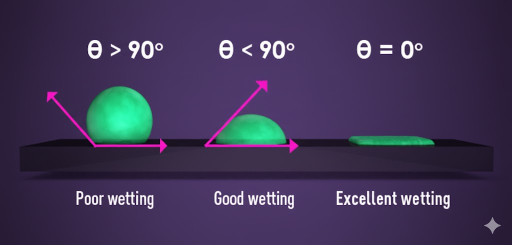
ENIG Wetting Issues: When Solder Refuses to Adhere
Poor solder wetting represents another prevalent challenge with ENIG finishes. Wetting describes the ability of molten solder to spread uniformly across the pad surface. When wetting is compromised, the solder may form uneven or incomplete joints, leading to significant reliability concerns. ENIG wetting issues often originate from surface contamination, oxidation of the nickel layer, or an excessively thick gold layer (above 0.05-0.1 micrometers), all of which can impede proper solder adhesion. Improper storage conditions can also exacerbate wetting problems. If ENIG-finished HDI PCBs are exposed to high humidity or significant temperature fluctuations for extended periods (e.g., over 6 months), the surface can degrade, diminishing its solderability.
ENIG Poor Solder Joint Formation: Compromised Connections
Weak or brittle solder joints are a direct consequence of underlying problems like black pad or inadequate wetting. In cases of ENIG poor solder joint formation, the solder may fail to bond correctly with the nickel layer, leading to joints that crack or fracture under thermal or mechanical stress. This issue is frequently observed in applications subject to high thermal cycling, where temperature variations induce expansion and contraction of materials. Industry studies indicate that solder joint failures in ENIG boards can increase by up to 30% if black pad or excessive phosphorus content is present. This statistic underscores the critical importance of addressing these fundamental issues during the manufacturing process to ensure the creation of robust and reliable connections.
ENIG Solder Paste Compatibility: Material Mismatch
Not all solder pastes are equally effective when used with ENIG finishes. ENIG solder paste compatibility issues arise when the flux or alloy composition within the paste does not interact optimally with the gold or nickel layers. For instance, certain lead-free solder pastes with high tin content (e.g., SAC305 alloy, comprising 96.5% tin) may form intermetallic compounds with the nickel layer that are overly brittle, leading to premature joint failures. Additionally, the flux in the solder paste must possess sufficient aggressiveness to effectively remove any surface oxides or contaminants present on the ENIG finish. If the flux is too mild, it may not adequately clean the surface, resulting in poor wetting and consequently, weak solder joints.
Practical Troubleshooting Steps for ENIG Solderability Problems
Now that the common issues have been identified, let's explore actionable solutions for troubleshooting ENIG solderability issues. These steps are designed to assist in diagnosing and resolving problems across the design, manufacturing, and assembly phases.
Diagnosing and Preventing ENIG Black Pad
Identification: Black pad is often imperceptible to the unaided eye until a soldering failure occurs. Employ a microscope to inspect pads for any discoloration or dark spots following soldering. A cross-sectional analysis can definitively reveal corrosion at the nickel-gold interface. Testing for phosphorus content using Energy Dispersive X-ray (EDX) analysis can also confirm if levels exceed the safe range of 7-9%.
Solution: To proactively prevent black pad, collaborate closely with your PCB fabricator to enforce stringent control over the ENIG plating process. This includes maintaining optimal pH levels (around 4.5-5.0) within the gold immersion bath and meticulously minimizing contamination. Specifying a lower phosphorus content in the nickel layer (targeting 7-8%) can also significantly reduce corrosion risks. If black pad is detected on finished boards, affected pads may require costly rework or replacement.
Addressing ENIG Wetting Issues
Identification: Poor wetting is evident when molten solder beads up or fails to spread uniformly across the pad during reflow. Conduct a visual inspection or utilize automated optical inspection (AOI) to detect non-wetted areas. Review storage conditions, as boards stored for over 6 months may exhibit reduced solderability due to surface degradation.
Solution: Ensure thorough cleaning of types of PCBs prior to soldering to remove contaminants such as fingerprints or dust. Employ a mild solvent or plasma cleaning if deemed necessary. Control the gold layer thickness to remain within 0.05-0.1 micrometers, as thicker layers can impede proper wetting. For extended storage, package boards in vacuum-sealed bags with desiccants to provide protection against humidity (ideal storage humidity is below 50% RH).
Rectifying ENIG Poor Solder Joint Formation
Identification: Weak solder joints can be identified through visual inspection (observing cracks or incomplete fillets) or by performing thermal cycling tests. A pull-test or shear-test can quantitatively assess joint strength; joints failing below 5-7 pounds of force typically indicate potential issues with the ENIG finish.
Solution: Address any underlying causes such as black pad or wetting issues by implementing the solutions outlined above. Optimize the reflow profile to ensure adequate heat (peak temperatures of 235-245°C for lead-free solder) and sufficient time above liquidus (60-90 seconds) to facilitate the formation of strong intermetallic bonds. If joints remain persistently weak, consider switching to an alternative surface finish for critical applications, although this should be a last resort due to the associated design changes.
Ensuring ENIG Solder Paste Compatibility
Identification: Compatibility issues typically manifest as poor wetting or brittle joints during the assembly process. Review the solder paste datasheet to ascertain its flux type (e.g., no-clean, water-soluble) and alloy composition. Conduct test samples on ENIG boards to observe joint quality before committing to full-scale production.
Solution: Select a solder paste with a flux that is specifically formulated to interact effectively with ENIG characteristics. For example, a mildly activated rosin (RMA) flux often works well with ENIG by efficiently cleaning the surface. Avoid overly aggressive fluxes that can corrode the delicate gold layer. If utilizing lead-free solder, ensure the alloy (e.g., SAC305) is compatible with nickel intermetallic formation—consult with your paste supplier for specific recommendations. Stencil design is also crucial; employ a stencil thickness of 0.1-0.15 mm to apply the correct volume of paste for consistent results.
Proactive Measures for Sustained ENIG Solderability Success
While troubleshooting is indispensable, prevention is ultimately more effective. Here are proactive steps to minimize ENIG solderability problems throughout the design and manufacturing lifecycle:
Collaboration and Process Optimization
Collaborate with Fabricators: Work intimately with your PCB manufacturer to establish and enforce stringent ENIG process parameters, including precise control over nickel phosphorus content (7-9%) and gold thickness (0.05-0.1 micrometers).
Specify Testing: Mandate incoming quality control tests, such as solderability testing in accordance with IPC-J-STD-003 standards, to thoroughly verify ENIG performance before commencing the assembly process.
Optimize Storage: Store ENIG-finished boards in carefully controlled environments (maintaining a temperature of 20-25°C and humidity below 50% RH) to preserve the integrity of the surface finish.
Review Assembly Processes: Ensure that reflow ovens are meticulously calibrated for consistent heating and consider utilizing nitrogen atmospheres if oxidation is a concern during the soldering phase.
Conclusion: Mastering ENIG for Dependable PCBs
ENIG continues to be a premier choice for PCB surface finishes, celebrated for its durability and versatility, yet it is not without its unique challenges. By thoroughly understanding and proactively addressing common ENIG solderability problems—such as the black pad phenomenon, wetting issues, compromised solder joint formation, and solder paste compatibility concerns—you can achieve consistently reliable and high-quality assemblies. Employ the troubleshooting steps and preventive measures detailed in this guide to confront issues head-on and significantly optimize your manufacturing processes.
Whether you are an engineer designing intricate boards or a manufacturer striving for zero-defect production, mastering ENIG troubleshooting is an invaluable skill. With meticulous attention to process control, judicious material selection, and refined assembly techniques, you can effectively minimize failures and ensure that your PCBs perform precisely as intended, even in the most demanding applications.