Introduction
Wave soldering remains a cornerstone process in through-hole PCB assembly, particularly for high-volume production where reliability under mechanical stress is critical. The PCB wave soldering double wave system represents an evolution, combining a turbulent first wave with a smooth laminar second wave to tackle the challenges of modern board designs. This setup addresses issues common in single-wave processes, such as incomplete wetting in dense pin fields and solder skips behind obstructing components. Electric engineers often encounter these complexities when integrating through-hole technology with surface-mount devices on mixed-technology boards. Understanding the PCB wave soldering double wave unlocks better defect reduction and process optimization. In this article, we explore its mechanics, advantages, and practical implementation.
What Is PCB Wave Soldering Double Wave and Why It Matters
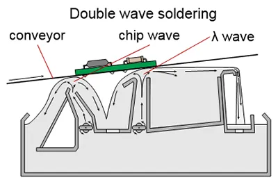
The PCB wave soldering double wave consists of two distinct solder waves generated from a molten solder pot: the initial turbulent wave, also called the chip wave, and the subsequent laminar wave. The turbulent wave creates an agitated flow that scrubs flux residues and drives solder into tight spaces around component leads. Following closely, the laminar wave delivers a stable, waterfall-like flow to refine the joints formed by the first wave. This dual approach matters because single-wave soldering struggles with high-density through-hole components, leading to inconsistent results in complex assemblies. For electric engineers designing boards with connectors or relays, the double wave ensures superior hole fill and joint integrity without excessive manual intervention.
This configuration aligns with industry requirements for solder joint quality as outlined in IPC-A-610, emphasizing acceptable criteria for wetting and fillet formation. As PCB densities increase, the double wave prevents common pitfalls like bridging from the turbulent phase being cleaned by the laminar phase. Engineers benefit from higher first-pass yields, reducing rework cycles in production lines. Ultimately, it supports scalable manufacturing for applications demanding robust electrical and mechanical performance.
Technical Principles Behind PCB Wave Soldering Chip Wave, Laminar Wave, and Turbulent Wave
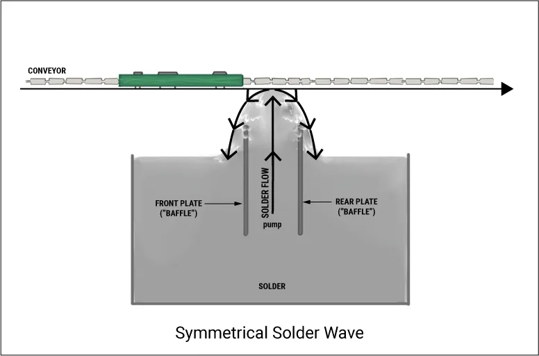
In the PCB wave soldering process, the turbulent wave operates through high-energy agitation, where solder is pumped to form a dynamic fountain that impacts the PCB underside with force. This action overcomes surface tension barriers, allowing flux-activated solder to penetrate plated through-holes and clean lead surfaces effectively. Flux, applied prior to preheating, removes oxides and promotes wetting, but the turbulent flow ensures it reaches shadowed or closely spaced pins. Transitioning to the laminar wave, the solder flow stabilizes into a flat, even crest, enabling controlled capillary action for vertical hole filling.
The interplay of these waves relies on precise fluid dynamics: turbulence disrupts stagnant flux layers, while laminar flow facilitates smooth PCB separation to drain excess solder. Heat transfer occurs rapidly during brief contact, with preheating ensuring flux activation and minimizing thermal gradients across the board. According to IPC J-STD-001, proper process control in such systems maintains solder joint cleanliness and strength. Engineers must consider board orientation, as aligning component leads perpendicular to the conveyor enhances solder distribution from both waves.
Wave height and conveyor speed further tune the contact dynamics, balancing penetration without splashing. This principle extends to mixed assemblies, where the chip wave handles surface-mount challenges before the laminar wave perfects through-hole joints.
Understanding and Mitigating the PCB Wave Soldering Shadow Effect
The PCB wave soldering shadow effect arises when taller components block the solder wave from reaching pads or leads positioned downstream along the conveyor direction. This creates unsoldered areas or poor wetting, often seen behind large capacitors or connectors in through-hole layouts. In single-wave systems, the smooth flow lacks the force to circumvent these obstacles, resulting in skips that fail IPC-A-610 acceptability standards. The double wave counters this effectively: the turbulent chip wave's agitation pushes solder into shadowed zones, disrupting air pockets and flux barriers.
Practical troubleshooting involves reorienting components so multi-lead devices face the wave directly, minimizing shadow length. Adequate spacing parallel to the flow allows the wave to reform between parts. For persistent issues, fixtures or pallets can shield sensitive areas while directing flow. The laminar wave then sweeps away any irregularities, ensuring downstream pads receive adequate solder volume.
Engineers should profile thermal gradients to confirm consistent activation across shadowed regions. Combining these strategies with flux selection per IPC J-STD-004 reduces non-wetting risks significantly.
Key Benefits of Implementing PCB Wave Soldering Double Wave
The primary benefit of the PCB wave soldering double wave lies in its ability to decouple wetting from joint finishing, yielding cleaner results than single-wave alternatives. Turbulent action excels at initial penetration for dense pin fields, reducing insufficient hole fill and cold joints. Subsequent laminar flow eliminates bridges, icicles, and burrs, streamlining post-soldering cleaning. This leads to higher process yields, especially for boards with varying component heights.
Reliability improves as joints exhibit better mechanical strength, crucial for vibrating environments or high-current paths. Cost savings emerge from fewer defects and less rework, making it ideal for medium-to-high volumes. Troubleshooting becomes straightforward, with defects traceable to specific wave interactions.
In mixed-technology flows, it complements reflow soldering by handling through-hole without disturbing surface-mounts. Overall, it enhances scalability while meeting stringent quality benchmarks.
Applications of PCB Wave Soldering Double Wave in Industry
PCB wave soldering double wave finds prime use in through-hole dominant assemblies like power supplies, automotive controls, and industrial controllers, where robust joints withstand thermal cycling. Mixed-technology boards benefit immensely, soldering surface-mount clips or drag solders after reflow without selective equipment. High-volume consumer electronics leverage its speed for connectors and relays that demand full barrel fill.
Engineers apply it in scenarios with pin densities beyond single-wave capacity, such as multi-row headers. For troubleshooting-focused production, it supports rapid iteration on shadow-prone layouts. Compliance with IPC-7530 for profiling ensures repeatability across batches.

Best Practices and Troubleshooting for Optimal Results
Start with board design: orient leads perpendicular to flow and space components to allow wave recovery. Select no-clean fluxes with balanced activity to survive both waves without excessive residues. Preheat uniformly to activate flux and prevent warping, monitoring profiles as per IPC-7530 guidelines.
Adjust conveyor tilt around 3 to 7 degrees for gravity-assisted drainage. For shadow effect troubleshooting, increase turbulent wave energy cautiously and verify with inspection. Use pallets for dual-sided boards to protect one side during soldering.
Regular pot skimming maintains solder purity, avoiding oxidized dross that hampers wetting. Post-process cleaning targets any laminar remnants. These practices minimize defects like bridging or skips systematically.
Conclusion
The PCB wave soldering double wave system, with its turbulent chip wave and laminar wave synergy, delivers reliable soldering for demanding through-hole and mixed assemblies. It effectively mitigates the shadow effect and other defects through targeted fluid dynamics, boosting yield and joint quality. Electric engineers gain practical tools for optimization, aligning with IPC standards for production excellence. By mastering these principles, teams achieve consistent results in high-stakes applications. Embrace this process for enhanced troubleshooting and performance.
FAQs
Q1: What distinguishes the PCB wave soldering chip wave from the laminar wave?
A1: The chip wave, or turbulent wave, uses agitation to clean leads and penetrate dense or shadowed areas, ensuring initial wetting. The laminar wave follows with smooth flow to remove excess solder, form clean fillets, and complete hole fill. This sequence prevents bridging while improving reliability in mixed assemblies. Proper sequencing aligns with IPC J-STD-001 for joint criteria.
Q2: How does PCB wave soldering double wave reduce the shadow effect?
A2: The turbulent first wave forces solder past tall components into downstream shadows, disrupting barriers that cause skips. Laminar flow then refines these joints without adding defects. Orient components perpendicular to the conveyor and space adequately for best results. This approach enhances wetting in complex layouts.
Q3: When should electric engineers choose PCB wave soldering turbulent wave setups?
A3: Opt for turbulent-inclusive double wave in high-density through-hole or mixed-tech boards prone to non-wetting. It excels where single laminar waves fail due to pin crowding or heights. Validate with thermal profiling to confirm flux activation. Ideal for volume production demanding IPC-A-610 compliance.
Q4: What are common troubleshooting steps for bridging in PCB wave soldering double wave?
A4: Check flux survival to the laminar wave and adjust conveyor speed for longer contact. Ensure perpendicular lead orientation to aid drainage. The second wave naturally clears turbulent excesses, but pallets help in persistent cases. Monitor for consistent preheating to avoid irregular flow.
References
IPC J-STD-001 — Requirements for Soldered Electrical and Electronic Assemblies. IPC, 2017
IPC-A-610H — Acceptability of Electronic Assemblies. IPC, 2019
IPC-7530 — Guidelines for Temperature Profiling for Mass Soldering Processes. IPC, 2008