What Exactly Are Trace Width Tolerances in PCB Manufacturing?
Trace width tolerance defines the permissible deviation from a conductor's intended width on a Printed Circuit Board (PCB). When you design a PCB, you specify a precise trace width to manage current flow, control impedance, or ensure signal integrity. However, during the intricate manufacturing process, various elements such as etching chemicals, copper layer thickness, and ambient conditions can induce minor discrepancies in the final trace width.
For illustration, if you specify a trace to be 10 mils (0.010 inches) wide, a tolerance of ±10% means the actual manufactured width could fall anywhere between 9 mils and 11 mils. While these variations might appear negligible, even small departures can profoundly impact performance in applications demanding high frequency or high current. A thorough understanding of these tolerances empowers you to engineer boards that maintain functionality despite inherent manufacturing inconsistencies.
Why Do Trace Width Variations Occur During PCB Manufacturing?
PCB manufacturing is a multi-stage process, and each step inherently carries the potential to introduce variations in trace width. Let’s examine the primary factors that contribute to these differences:
1. Etching Process Variations
The etching procedure involves chemically removing unwanted copper to form the circuit traces. Yet, variables such as the etchant's chemical concentration, temperature, and the duration of exposure can lead to either over-etching or under-etching. Over-etching results in traces that are narrower than specified, whereas under-etching leaves them wider. Standard etching processes commonly yield trace width tolerances ranging from ±10% to ±15%.
2. Influence of Copper Thickness
The initial thickness of the copper layer on a PCB directly affects the amount of material that needs to be removed during etching. Thicker copper (e.g., 2 oz/ft² or 70 μm) generally allows for superior control over trace width, which in turn helps reduce tolerance variations. Conversely, thinner copper (e.g., 0.5 oz/ft² or 17.5 μm), often employed in high-density designs, can result in greater deviations due to the more pronounced impact of the etching process on finer traces.
3. Quality of Artwork and Masking
The integrity of the design artwork and the precision of the photomask utilized in manufacturing are paramount. If the artwork contains imperfections or the mask alignment is inaccurate, the resulting traces may deviate from the original design specifications. High-resolution design files and meticulous masking techniques are crucial for minimizing these issues, allowing for tolerances closer to ±10%.
4. Precision of Manufacturing Equipment
The tools and machinery deployed in the production environment exhibit varying levels of precision. State-of-the-art manufacturing facilities equipped with modern machinery can achieve significantly tighter tolerances, often below ±10%. In contrast, older or less precise setups may result in broader variations, potentially extending up to ±20%.
What Constitutes an Acceptable Trace Width Range?
The definition of an acceptable trace width range is contingent upon the specific application, the design’s requirements, and the manufacturer’s capabilities. Here are some general guidelines applicable to various common scenarios:
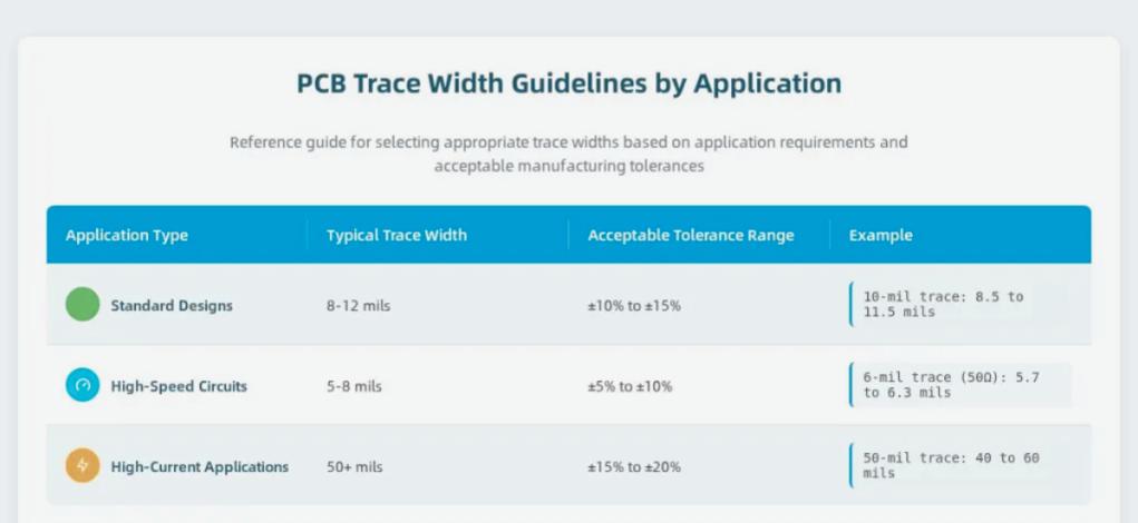
● Standard Designs: For general-purpose PCBs, a tolerance of ±10% to ±15% is typically considered acceptable. For a 10-mil trace, this translates to an actual width ranging from 8.5 to 11.5 mils.
● High-Speed Circuits: In designs where signal integrity is absolutely critical, such as those operating at frequencies exceeding 100 MHz, tighter tolerances (e.g., ±5% to ±10%) are preferred to maintain consistent impedance. A 50-ohm impedance trace, for instance, might necessitate a nominal width of 6 mils with a maximum deviation of only ±0.3 mils.
● High-Current Applications: For power distribution circuits handling currents above 5A, wider traces (e.g., 50 mils or more) are standard. In these cases, a tolerance of ±15% to ±20% might still be deemed acceptable, as minor width variations have a proportionally smaller impact on overall performance.
It is always advisable to consult directly with your manufacturing partner to ascertain their specific capabilities. Certain advanced processes, such as those utilized for high-density interconnect (HDI) boards, can achieve tolerances as tight as ±5%, whereas standard processes might typically hover around ±15%.
How Do Trace Width Variations Impact PCB Performance?
Even minor deviations in trace width can profoundly influence a PCB’s operational performance. Here’s a breakdown of how these variations affect critical aspects of your design:
1. Signal Integrity
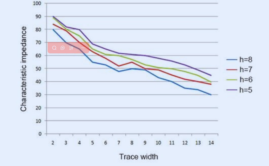
In high-speed designs, trace width directly dictates the characteristic impedance. A variation of just 1 mil in a 6-mil trace can alter the impedance by several ohms, potentially inducing signal reflections and leading to data errors. For example, a trace designed for 50-ohm impedance could shift to 55 ohms if it is narrower than intended during manufacturing, severely compromising signal integrity at frequencies exceeding 200 MHz.
2. Current Carrying Capacity
The trace width determines the maximum current a PCB can safely conduct without overheating. A trace that is unexpectedly narrower reduces its current capacity, potentially leading to excessive heat generation (e.g., a temperature rise of 20°C or more) and eventual failure. For instance, a 20-mil trace designed for 2A might only be able to safely handle 1.5A if its width is reduced to 18 mils due to manufacturing variations.
3. Voltage Drop
Narrower traces inherently possess higher electrical resistance, which results in greater voltage drops across the trace. In power delivery networks, this can lead to components receiving insufficient voltage, thereby adversely affecting their proper operation. A 10% reduction in trace width can proportionally increase resistance by approximately 11%, exacerbating voltage drop issues.
Quality Control Measures for Trace Width Tolerances in PCB Manufacturing
Rigorous quality control is indispensable for ensuring that trace width variations remain strictly within acceptable limits. Here are the key steps manufacturers implement to maintain tight tolerances, along with how you, as a designer, can contribute to this process:
1. Automated Optical Inspection (AOI)
Manufacturers deploy Automated Optical Inspection (AOI) systems to meticulously scan PCBs and precisely measure trace widths post-etching. These advanced systems are capable of detecting deviations as minuscule as 0.5 mils, thereby guaranteeing that traces conform to the specified tolerance range. Regular calibration of AOI equipment is critical for achieving consistently accurate results.
2. Comprehensive Process Control and Monitoring
Strict control over process variables such as etchant concentration, temperature, and etching time is crucial for minimizing variations. Advanced manufacturing facilities continuously monitor these parameters in real-time, making instantaneous adjustments to processes to maintain trace widths within a narrow ±10% of the design specification.
3. Adherence to Design for Manufacturability (DFM) Guidelines
As a designer, you play a pivotal role by diligently adhering to Design for Manufacturability (DFM) guidelines. Avoid specifying trace widths below the manufacturer’s absolute minimum capabilities (often 3-5 mils for standard processes) unless absolutely necessary. Provide clear and precise design files with unambiguously defined trace widths and spacing to mitigate artwork-related errors.
4. Collaborative Engagement with Manufacturers
Engage in proactive communication with your large PCB manufacturer early in the design phase. Clearly articulate your tolerance requirements, especially for critical traces, and explicitly confirm their production capabilities. For high-speed designs, request comprehensive impedance testing to verify that manufactured trace widths align with the target range for your desired impedance (e.g., 50 ohms ±5%).

How to Effectively Specify Trace Width Tolerances in Your PCB Design
To guarantee your PCB performs exactly as intended, it is crucial to explicitly specify trace width tolerances within your design documentation. Follow these steps to communicate your requirements clearly and effectively:
● Designate Critical Traces: Identify all traces where tight tolerances are absolutely essential, such as those forming high-speed signal paths or critical power delivery lines. Clearly note the required tolerance (e.g., ±5% for a 6-mil trace).
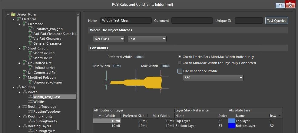
● Utilize Design Software Features: Most professional PCB design software packages offer functionalities to establish trace width rules and tolerances. Leverage these features to automatically flag traces that demand precision.
● Embed Notes in Fabrication Files: Include detailed notes within your Gerber files or fabrication drawings, explicitly specifying acceptable ranges for critical trace widths (e.g., "10 mils ±1 mil for all high-speed data lines").
● Solicit Manufacturer Feedback: Share your complete design files with the manufacturer well in advance of production to confirm whether your specified tolerances are genuinely achievable with their current processes and equipment.
By taking these proactive measures, you can significantly reduce the risk of performance degradation stemming from unwanted trace width variations.
Practical Tips for Minimizing Trace Width Variations in Your PCB Designs
While some degree of manufacturing variation is often unavoidable, you can implement several strategies to minimize their impact on your PCB's performance. Here are practical tips to consider:
● Incorporate Design Margin: Where feasible, design traces slightly wider than the absolute minimum required. This provides a buffer to accommodate potential narrowing that might occur during the manufacturing process. For example, if a 2A current requires a 10-mil trace, consider using a 12-mil trace if space permits.
● Select Appropriate Copper Weight: Opt for a thicker copper layer (e.g., 1 oz/ft² or 35 μm) as it generally offers better control during etching and consequently results in reduced tolerance variations.
● Avoid Unduly Tight Tolerances: Unless strictly necessary for critical performance, refrain from specifying tolerances that are significantly tighter than the manufacturer's standard capabilities. Overly tight tolerances can lead to increased manufacturing costs without providing proportional performance benefits.
● Conduct Prototype Testing: For designs deemed critical, order a small batch of proto PCB boards. Meticulously measure the actual trace widths and rigorously test the electrical performance (e.g., impedance, current handling) before committing to full-scale production.
Conclusion: Mastering Trace Width Tolerances for Superior PCBs
A profound understanding of trace width tolerances in PCB manufacturing is a cornerstone for designing boards that are both reliable and high-performing. Variations in trace width, commonly ranging from ±10% to ±20%, can critically affect signal integrity, current carrying capacity, and voltage drop. Therefore, it is imperative to account for these variations during the design phase. By accurately understanding the acceptable trace width range for your specific application, fostering close collaboration with manufacturers, and adhering to stringent quality control protocols, you can confidently ensure your PCBs meet or exceed performance expectations.
Whether your project involves a high-speed circuit demanding tight tolerances of ±5% or a power distribution board where ±15% is acceptable, meticulous planning and effective communication with your manufacturing partner are absolutely crucial. Keep these comprehensive insights in mind as you embark on your next PCB design, and you will be exceptionally well-equipped to expertly navigate the inherent challenges of manufacturing variations.
AIVON is deeply committed to empowering your projects with precision manufacturing and expert guidance. By prioritizing rigorous quality control and implementing advanced manufacturing processes, we strive to minimize trace width variations, delivering circuit boards that precisely match your specifications. Commence your next project with unwavering confidence, knowing that every intricate detail, down to the minutest trace, is handled with unparalleled care and precision.