Introduction
In the realm of PCB manufacturing, double-sided PCBs represent a foundational technology used across countless electronic applications, from consumer devices to industrial controls. These boards feature conductive copper layers on both sides connected via plated through-holes, enabling more complex circuitry than single-sided designs. Ensuring rigorous quality control and testing procedures is essential to prevent defects that could lead to field failures, increased rework costs, or safety risks. Double-sided PCB quality control encompasses inspections and tests throughout the production process, aligning with established industry standards to guarantee reliability. This article explores key procedures, methods like AOI and ICT, and best practices tailored for electrical engineers involved in design verification and procurement.
Understanding Double-Sided PCBs and the Need for Quality Control
Double-sided PCBs consist of a substrate with copper foil laminated on both surfaces, where vias provide electrical interconnections between layers. Unlike multilayer boards, they lack internal planes, making them cost-effective for moderate complexity circuits but susceptible to specific fabrication challenges such as via plating inconsistencies or board warpage. Quality control in double-sided PCB manufacturing matters because even minor defects, like drill breakout or insufficient plating thickness, can compromise signal integrity or mechanical stability under thermal stress. Comprehensive PCB testing and inspection mitigate these risks, reducing yield losses and ensuring compliance with performance specifications. Factory-driven approaches emphasize early detection to streamline production and support high-volume runs.
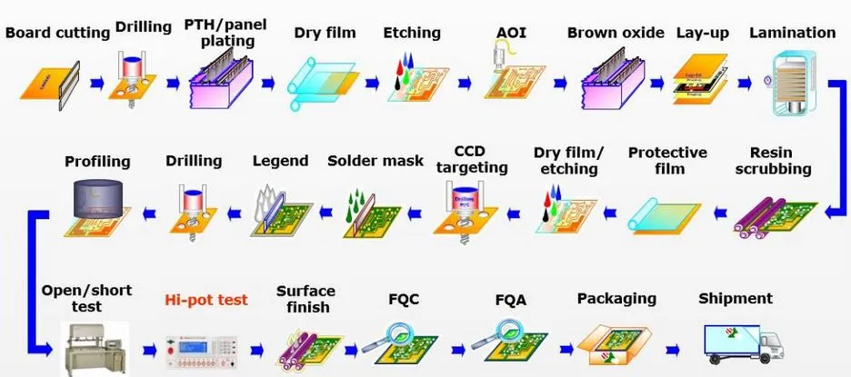
Key Stages of Quality Control in Double-Sided PCB Manufacturing
Quality control begins with incoming material inspection, where substrates, copper foils, and chemicals are verified for specifications such as thickness tolerance and cleanliness. During fabrication, drilling accuracy is checked to ensure hole sizes meet design requirements, preventing issues like aspect ratio violations in plated through-holes. After electroless and electrolytic plating, cross-sections are examined for copper thickness uniformity, typically targeting 25 microns minimum in holes per standard guidelines. Etching processes follow, with post-etch inspections confirming trace width and spacing adherence. Solder mask application and silkscreen printing undergo visual and automated checks for coverage and legibility. Final bare board electrical testing confirms continuity and isolation before packaging.
Suggested Reading: Essential Techniques for Soldering Through-Hole Components on Double-Sided PCBs
Essential PCB Inspection Methods
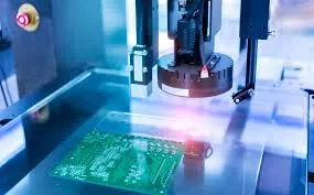
PCB inspection starts with manual visual checks using magnification tools to identify surface defects like scratches, contamination, or mask voids. Microscopic examination reveals finer issues such as pitting in plating or fiber prominence on laminate surfaces. Automated Optical Inspection (AOI) revolutionizes this process by employing high-resolution cameras and pattern recognition software to scan for deviations in traces, pads, and vias at production speeds. AOI excels in detecting opens, shorts, and dimensional errors on double-sided boards, comparing actual images against golden samples or CAD data. For hidden features, X-ray inspection complements AOI by revealing via fill quality and barrel cracks. These methods ensure double-sided PCB quality control aligns with visual acceptability criteria.
In practice, AOI systems are programmed for specific defect types common to double-sided manufacturing, such as mouse bites in edges or excessive solder mask encroachment. Engineers benefit from integrating AOI at multiple stages, including post-etch and post-solder mask, to catch progressive issues early. For a deeper look at how AOI detects defects across both sides, see our guide on AOI equipment for PCB quality control.
Critical PCB Testing Procedures
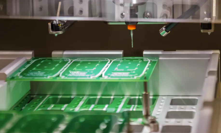
Electrical testing forms the backbone of PCB testing, verifying functionality before assembly. In-Circuit Testing (ICT), often using bed-of-nails fixtures, probes nets to measure continuity, shorts, resistance, and capacitance on populated boards. For bare double-sided PCBs, flying probe testers offer flexibility without custom fixtures, ideal for prototypes or low volumes. These tests detect opens in vias or plating delamination that inspections might miss. Functional testing simulates operational conditions, powering the board to confirm signal paths and timing. Thermal stress tests, including temperature cycling, assess warpage and delamination risks under expansion mismatches.
ICT fixtures are designed with precision pogo pins matched to via locations, ensuring reliable contact on both board sides. According to IPC-A-600, acceptability criteria guide these tests by defining allowable imperfections in conductor integrity.
Advanced Testing for Reliability Assurance
Beyond basic electrical checks, reliability testing evaluates long-term performance. Warpage measurement uses tools like shadow moiré or dial gauges to quantify bow and twist, critical for double-sided boards prone to asymmetry. Ionic contamination testing via resistivity probes detects flux residues that could cause dendrite growth. Solderability tests preserve sample coupons through the process, dipping them to verify wetting characteristics. Cross-sectional analysis, though destructive, provides definitive plating and hole wall integrity data. These procedures support qualification per IPC-6012 specifications for rigid printed boards.
Best Practices for Double-Sided PCB Quality Control
Implement a layered quality approach, starting with design for manufacturability reviews to flag via densities or drill sizes that challenge fabrication. Standardize inspection protocols across shifts, training operators on IPC class levels appropriate for the application, such as Class 2 for dedicated service electronics. Integrate AOI and ICT data into statistical process control charts to track defect trends and adjust parameters like plating bath chemistry proactively. Maintain cleanroom conditions during handling to minimize contamination, and use automated handling to reduce mechanical damage. Collaborate with suppliers on material certificates, ensuring laminates meet minimum Tg ratings for thermal stability. Regular audits of equipment calibration sustain test accuracy.
Document all non-conformances with root cause analysis, feeding insights back into process improvements. For high-reliability needs, incorporate burn-in testing post-assembly.
Common Defects and Troubleshooting in Double-Sided PCBs
Double-sided boards commonly exhibit plating voids from poor activation or air entrapment during electroless plating, detectable via X-ray or cross-section. Delamination arises from moisture in laminates or over-etching, addressed by pre-bake drying and controlled etchants. Annular ring reductions occur from drill wander, mitigated by precise CNC drilling and pilot holes. Solder mask registration errors lead to exposed copper, caught early by AOI. Warpage from uneven copper distribution requires balanced patterning or constrained baking. Troubleshooting involves isolating defects through sequential testing, correlating with process logs for corrections.
Conclusion
Effective double-sided PCB quality control integrates inspections like AOI and tests such as ICT across manufacturing stages to deliver reliable boards. By adhering to standards and best practices, engineers minimize defects, enhance yield, and ensure end-product performance. Prioritizing factory-driven procedures not only meets specifications but also supports scalable production. Electrical engineers should specify these protocols in procurement to align vendor capabilities with design intent.
FAQs
Q1: What is AOI in double-sided PCB quality control?
A1: AOI, or Automated Optical Inspection, uses cameras and algorithms to detect visual defects like trace discontinuities or pad misalignment on double-sided PCBs. It operates post-etch and post-mask, comparing boards to reference data for high-speed verification. This method surpasses manual inspection in consistency, reducing human error in PCB manufacturing. Integration of AOI ensures early defect capture, improving overall quality control efficiency.
Q2: How does ICT contribute to PCB testing?
A2: In-Circuit Testing (ICT) employs fixtures to probe electrical nets, checking for opens, shorts, and component values on assembled double-sided PCBs. It verifies via connectivity and passive elements, essential after SMT processes. Unlike flying probe, ICT suits high-volume runs with custom beds. Proper fixturing prevents board stress, aligning with standards for reliable PCB testing outcomes.
Q3: Why is visual inspection fundamental in PCB inspection?
A3: Visual inspection identifies surface anomalies like contamination or mask defects on double-sided boards using aids like stereomicroscopes. It serves as the first quality gate per IPC guidelines, before advanced AOI. Trained inspectors classify issues by severity, enabling quick disposition. Combining it with automated methods provides comprehensive double-sided PCB quality control.
Q4: What role do standards play in double-sided PCB manufacturing?
A4: Standards like IPC-A-600 define acceptability criteria for features such as hole walls and conductors, guiding inspections and tests. They ensure uniformity across facilities, minimizing variability in double-sided PCB quality control. Compliance verifies performance for applications, from consumer to aerospace. Engineers reference them for spec sheets and audits.
References
IPC-A-600K — Acceptability of Printed Boards. IPC, 2020
IPC-6012E — Qualification and Performance Specification for Rigid Printed Boards. IPC, 2017
IPC J-STD-001H — Requirements for Soldered Electrical and Electronic Assemblies. IPC, 2018