Introduction
Heavy copper double-sided PCBs represent a robust solution for demanding power electronics applications where high current handling is essential. These boards feature thick copper layers on both sides of the substrate, typically exceeding standard thicknesses to support elevated electrical loads without excessive heating or voltage drop. Electrical engineers often select them for power supplies, motor drives, and inverters due to their balance of performance and manufacturability. Double-sided configurations allow routing on both surfaces, optimizing space while leveraging heavy copper's inherent strengths. This article explores the key advantages, drawing from established engineering principles and manufacturing insights to guide PCB design decisions.
What Are Heavy Copper Double-Sided PCBs and Why Do They Matter?
Heavy copper double-sided PCBs consist of a dielectric core with copper foil thicknesses greater than 3 ounces per square foot on each side, enabling them to function as high current PCBs in power-intensive circuits. Unlike standard 1-ounce copper boards, these designs accommodate currents that would overwhelm thinner traces, making them critical for applications like welding equipment and automotive power modules. The double-sided layout provides two conductive planes for current paths, signal routing, and ground returns, which enhances overall circuit efficiency compared to single-sided alternatives. In PCB manufacturing, this approach simplifies production relative to multilayer stacks while delivering comparable thermal and mechanical performance.
The relevance stems from the growing demand for compact, reliable power PCBs in renewable energy systems and electric vehicles. Engineers prioritize these boards to minimize I-squared-R losses and thermal hotspots, ensuring longevity under cyclic loading. Factory processes for heavy copper double-sided PCBs align with IPC-6012 specifications for rigid board qualification, guaranteeing consistent copper plating and etching uniformity. As power densities increase, selecting double-sided heavy copper becomes a strategic choice for balancing cost, reliability, and space constraints.
Technical Principles Behind the Advantages
Heavy copper double-sided PCBs excel in current-carrying capacity because thicker copper reduces trace resistance, allowing higher amperage without significant voltage drops or overheating. For instance, a 4-ounce trace can handle several times the current of a 1-ounce equivalent at the same width, distributing load across both board sides for balanced flow. This dual-layer setup also facilitates parallel current paths, further lowering impedance in power PCB designs. Electrical engineers benefit from predictable performance, as current ratings follow guidelines in IPC-2221 for trace width and spacing.
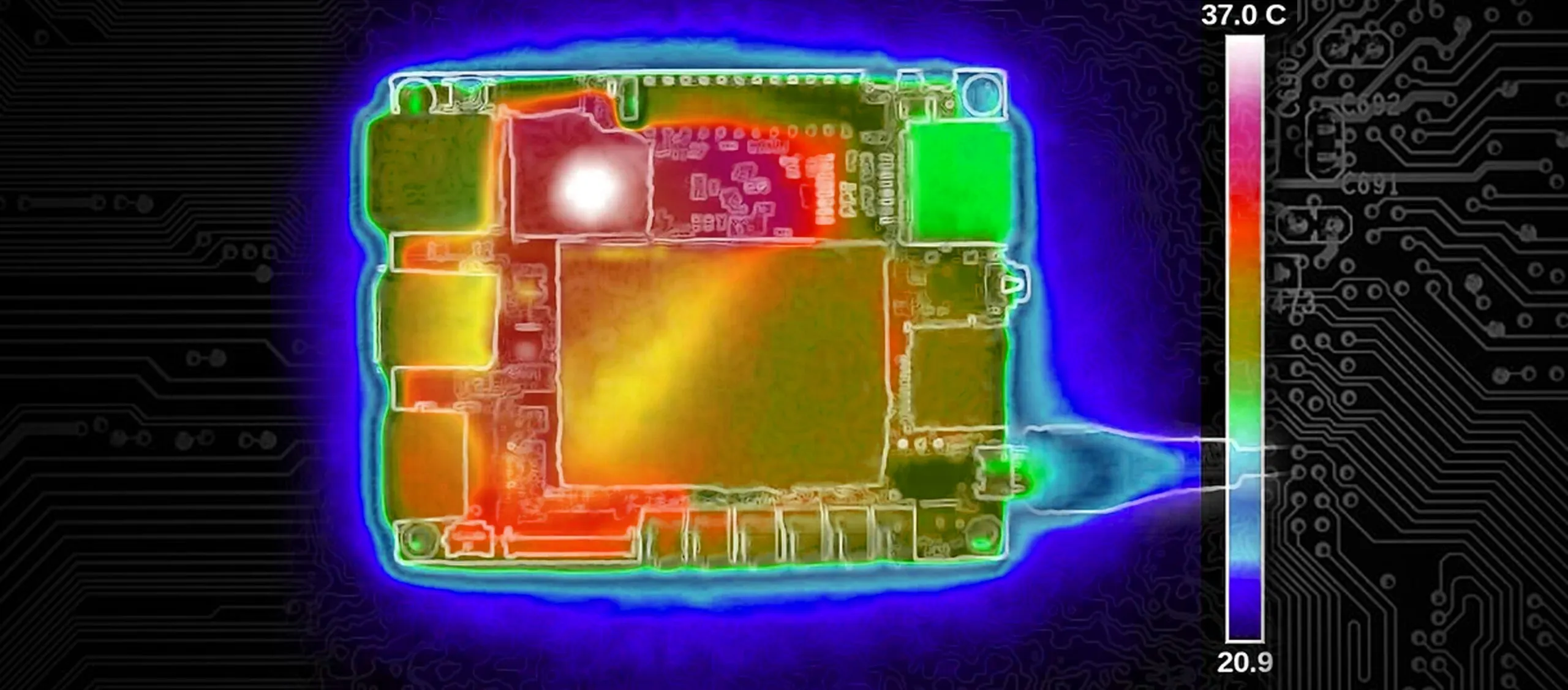
Thermal management improves markedly with heavy copper, as the increased cross-sectional area acts as an integrated heat spreader, dissipating joule heating more effectively than thin copper layers. In double-sided configurations, heat from components on one side conducts through the copper plane to the opposite surface or edges, reducing peak temperatures during high current operation. This intrinsic dissipation often eliminates the need for additional heatsinks, simplifying assembly and improving reliability in enclosed environments. Manufacturing insights reveal that uniform plating on both sides prevents hotspots, aligning with thermal stress tests per industry standards.
Mechanically, heavy copper double-sided PCBs offer superior durability against vibration, thermal cycling, and physical stress due to the reinforced structure from thick foils. The dual layers provide balanced rigidity, minimizing warpage during soldering or operation compared to unbalanced single-sided heavy copper boards. This stability supports via plating integrity and solder joint strength, crucial for high current PCB applications exposed to mechanical loads. Engineers note that the thicker copper resists cracking under flexure, extending service life in rugged environments.
Cost and layer efficiency represent another core advantage, as double-sided heavy copper avoids the complexity and expense of multilayer lamination. Fabricating four or more layers with heavy copper demands precise press cycles and alignment, driving up PCB manufacturing costs significantly. In contrast, double-sided designs streamline etching, plating, and drilling, yielding faster turnaround times suitable for prototyping or medium-volume production. This efficiency suits power PCBs where routing density remains moderate, allowing wide traces on both sides without interlayer vias.
Best Practices for PCB Design and Manufacturing
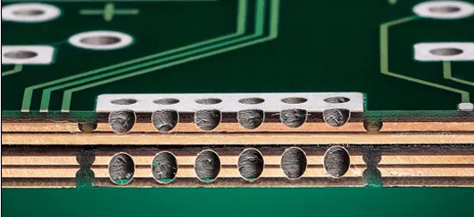
In PCB design for heavy copper double-sided boards, engineers should calculate trace widths using IPC-2152 charts, accounting for temperature rise and ambient conditions to ensure safe current densities. Wider traces and filled planes on both sides optimize current distribution, while maintaining minimum spacing to prevent arcing under voltage stress. Vias require heavier plating, often 2 mils or more, to match layer capabilities and avoid bottlenecks in high current paths. Logical component placement groups high-power elements centrally, leveraging the board's thermal mass for even dissipation.
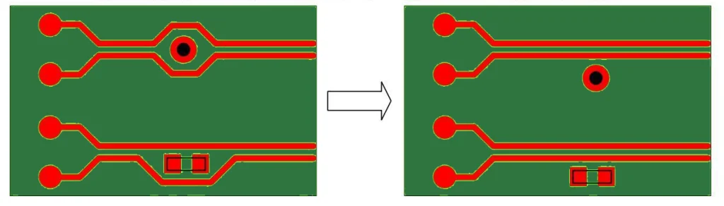
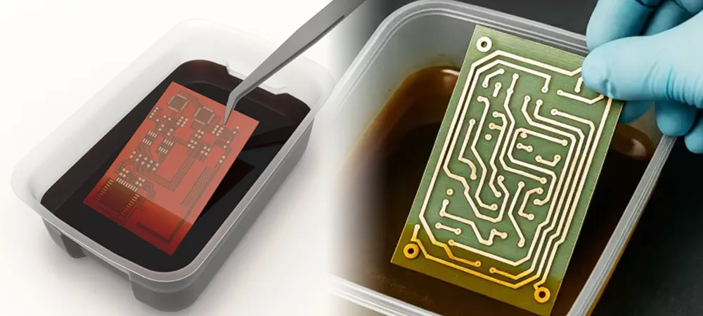
During manufacturing, sequential lamination or differential etching techniques control copper buildup on inner edges, preventing shorts in dense areas. Prepreg selection must match the copper weight to avoid delamination under thermal expansion mismatch. Solder mask application demands thicker formulations to cover heavy copper topography without voids. Quality checks per IPC-A-600 ensure external copper meets thickness tolerances, typically plus or minus 10 percent.
For assembly, engineers recommend reflow profiles adjusted for the board's mass, with extended preheat to minimize shock. Through-hole components benefit from oversized pads to accommodate copper expansion. Testing involves current load simulations to verify temperature profiles match design predictions. These practices enhance yield and reliability in power PCB production.
Key Applications and Practical Insights
Power conversion systems, such as DC-DC converters and battery management units, frequently employ heavy copper double-sided PCBs for their ability to handle pulsed high currents without degradation. In these scenarios, the dual sides enable separate power and control routing, reducing crosstalk while maximizing copper pour areas for grounding. Factory data indicates lower failure rates in thermal cycling tests compared to standard copper equivalents.
Troubleshooting common issues, like uneven plating, involves verifying electroplating bath chemistry and current density uniformity across the panel. Warpage in heavy copper boards arises from asymmetric cooling, mitigated by controlled bake-out and fixture support during fabrication. Engineers can simulate these effects early in design to preempt problems.
Conclusion
Heavy copper double-sided PCBs deliver compelling advantages in current capacity, thermal performance, mechanical robustness, and cost-efficiency for high current and power applications. Their simpler structure facilitates reliable PCB design and manufacturing without sacrificing functionality. By adhering to standards like IPC-2221 and IPC-6012, engineers achieve optimized outcomes tailored to demanding environments. Selecting this configuration empowers innovative solutions in power electronics, balancing performance with practicality.
FAQs
Q1: What defines a heavy copper double-sided PCB?
A1: A heavy copper double-sided PCB features copper thicknesses exceeding 3 ounces per square foot on both layers, ideal for high current PCB needs. This setup supports elevated amperage through reduced resistance and dual routing paths. Manufacturing follows rigid board specs to ensure plating uniformity and etch control. Engineers use it where power density requires robust traces without multilayer complexity.
Q2: Why choose double-sided over multilayer for heavy copper power PCBs?
A2: Double-sided heavy copper designs cut costs and simplify PCB manufacturing by avoiding lamination steps, while providing sufficient current paths for many applications. They offer better thermal spreading across planes compared to thin multilayer copper. Mechanical stability improves with balanced layers, reducing warpage risks. This makes them preferable for medium-complexity power PCBs focused on reliability.
Q3: How does heavy copper improve thermal management in double-sided PCB design?
A3: Heavy copper's thickness in double-sided configurations conducts heat away from hotspots more effectively, lowering peak temperatures under high current loads. Both sides act as spreaders, enhancing dissipation to edges or components. Design best practices include wide pours and via stitching for flux transfer. This aligns with standards for thermal reliability in power electronics.
Q4: What are key manufacturing challenges for heavy copper double-sided PCBs?
A4: Challenges include differential etching to maintain trace geometry and plating uniformity on thick foils during PCB manufacturing. Warpage control requires matched materials and fixturing. Standards guide tolerances for external copper finish. Addressing these ensures high yields for high current applications.
References
[1] IPC-2221B — Generic Standard on Printed Board Design. IPC, 2003
[2] IPC-6012E — Qualification and Performance Specification for Rigid Printed Boards. IPC, 2017
[3] IPC-2152B — Standard for Determining Current Carrying Capacity in Printed Board Design. IPC, 2009