Introduction
RF and microwave engineers require materials that maintain signal integrity at frequencies extending into the GHz range. Taconic PCBs, leveraging specialized laminates, deliver low insertion loss and dielectric stability essential for such demanding applications. This guide explores Taconic PCB design rules, stack-up strategies, and layout techniques to optimize performance in high frequency PCB design. Engineers can apply these principles to reduce signal distortion and enhance reliability in radar systems, antennas, and communication modules. By following structured approaches, designs achieve controlled impedance and minimal crosstalk. The content draws on established engineering practices for microwave PCB design.
Why Taconic Materials Matter for RF and Microwave Applications
Taconic laminates feature low dissipation factors and consistent dielectric constants across broad frequency bands. These properties minimize signal attenuation, critical for maintaining phase linearity in microwave circuits. Moisture absorption remains low, preventing shifts in electrical performance during environmental exposure. Thermal stability supports operation under power dissipation without dimensional changes that could alter impedance. Engineers select Taconic materials for applications like phased array radars where precision is paramount. Compliance with IPC-6018 ensures qualification for high frequency (microwave) printed boards.
In RF PCB layout guidelines, the uniform thickness profiles of Taconic substrates facilitate repeatable manufacturing. This consistency aids in predicting electromagnetic behavior during simulation. Low loss tangents reduce heat generation, allowing higher power handling in amplifiers. Designers benefit from tight tolerances in dielectric properties, simplifying stack-up planning. Overall, these attributes position Taconic PCBs as a reliable choice for high frequency PCB design. Compare Taconic with other low-Dk options in our Low Dk PCB Materials Comparison Guide.
Core Technical Principles of Taconic PCB Design
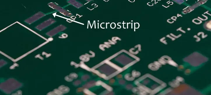
Transmission line theory governs signal propagation on Taconic PCBs, where characteristic impedance depends on trace geometry and substrate properties. Microstrip and stripline configurations exploit the low dielectric constant for wideband performance. Field fringing effects demand precise control of ground plane proximity to avoid unwanted coupling. Via transitions introduce discontinuities that require compensation through stub tuning or back-drilling. Engineers model these using quasi-TEM approximations valid up to several GHz. Adhering to IPC-2221 generic standard on printed board design provides foundational rules for spacing and clearance.
Skin effect confines currents to conductor surfaces at microwave frequencies, emphasizing the need for smooth copper profiles. Dielectric losses scale with frequency squared, underscoring the value of Taconic's low loss materials. Thermal expansion mismatch between copper and substrate influences reliability in multilayer builds. Controlled impedance traces maintain return loss below acceptable thresholds. These principles form the basis for Taconic PCB design rules in RF environments.
Essential Taconic PCB Design Rules
Taconic PCB design rules prioritize impedance control, typically targeting 50 ohms for single-ended lines. Trace width and spacing follow 3H rules, where H is substrate height, to suppress crosstalk. Minimum spacing equals three times the trace width for microstrip lines. Vias use stitching along signal paths at lambda/20 intervals to contain fields. Ground planes cover entire layers beneath RF signals, with clearance for non-RF components. These rules align with RF PCB layout guidelines for minimal radiation.
Component placement groups RF sections away from digital circuitry to avoid noise injection. Power distribution employs decoupled planes with via fences. Solder mask thickness remains thin over transmission lines to preserve impedance. Fabrication tolerances demand specification of drill parameters, such as 130-degree point carbide bits for clean holes. Engineers verify designs against IPC-2252 for RF/microwave circuit boards. Following these ensures robust Taconic PCB design rules implementation.
Building Effective Taconic PCB Stack-up
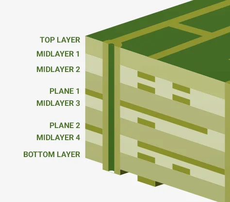
Taconic PCB stack-up begins with symmetric layering to prevent warpage from CTE differences. Core and prepreg selection matches dielectric constants for uniform fields. Signal layers pair with adjacent ground planes for return path integrity. Typical four-layer stack features signal-ground-core-ground-signal. Thickness control achieves target impedance, often 0.127 mm dielectric for 50-ohm microstrip. Hybrid stacks combine Taconic with FR4 for cost in non-critical areas.
Plane splitting avoids under components to maintain shielding. Via aspect ratios stay below 10:1 for plating uniformity. Thermal vias enhance heat dissipation from active devices. Stack-up planning tools simulate fields, confirming isolation between layers. Microwave PCB design benefits from thin dielectrics reducing radiation losses. Engineers iterate stack-ups to balance electrical and mechanical needs. For cost-optimized high-frequency designs using Taconic, see Cost Effective High Frequency PCB Design with Taconic Materials.
RF PCB Layout Guidelines for Taconic Substrates
RF PCB layout guidelines emphasize contiguous ground pours surrounding transmission lines. Coplanar waveguide (CPW) configurations leverage upper ground for balanced fields on Taconic. Bends use curved traces with radius at least 3W to minimize reflections. Decoupling capacitors place within lambda/4 of IC pins. Partitioning isolates LO, RF, and IF paths with grounded guards. These practices uphold Taconic PCB design rules for low VSWR
Length matching preserves phase alignment in differential pairs. Avoid right angles in routing to reduce stub effects. Shielding cans cover sensitive areas, grounded multiply. Test points employ 0-ohm resistors for non-invasive probing. Layout symmetry aids manufacturability. High frequency PCB design thrives on these disciplined approaches.
Best Practices in Microwave PCB Design with Taconic
Microwave PCB design with Taconic focuses on minimizing transitions between line types. Tapered sections match impedances at microstrip-to-stripline shifts. Back-drilling removes stubs longer than lambda/20. Enclosures integrate with PCB edges for seamless shielding. Power amplifier layouts radial star grounding from die. Thermal management uses embedded heat spreaders compatible with low-loss dielectrics.
Surface finishes like ENIG preserve skin effect performance without oxidation. Bake-out procedures remove absorbed moisture pre-assembly. Fixture designs support precise alignment during testing. These best practices elevate microwave PCB design outcomes. Troubleshooting involves TDR measurements for discontinuity hunting.
High Frequency PCB Design Considerations
High frequency PCB design extends Taconic capabilities to mmWave with submicron tolerances. Material stability over temperature prevents detuning. Multilayer transitions employ blind/buried vias for density. EMC compliance demands Faraday cage-like pours. Simulation validates pre-layout predictions. Fabrication feedback refines iterations. Explore advanced layout techniques in High Frequency PCB Layout Techniques for Satellite Communication Systems.
Conclusion
Taconic PCBs enable superior RF and microwave performance through tailored design rules and stack-ups. Implementing RF PCB layout guidelines ensures signal fidelity and low loss. Microwave PCB design best practices address unique challenges like via parasitics. High frequency PCB design demands precision in every layer. Engineers achieve reliable outcomes by integrating these strategies systematically.
FAQs
Q1: What are the primary Taconic PCB design rules for RF applications?
A1: Taconic PCB design rules emphasize 50-ohm impedance control, 3x trace width spacing for microstrips, and dense via stitching along signals. Ground planes must fully cover RF areas with no splits under traces. These rules minimize crosstalk and radiation per standard RF practices. Compliance reduces return loss effectively.
Q2: How should I plan a Taconic PCB stack-up for microwave PCB design?
A2: Taconic PCB stack-up requires symmetric layers with signal-ground pairing for low inductance returns. Dielectric thicknesses target precise impedance, often using thin cores. Hybrid materials handle mixed signals cost-effectively. Verify with field solvers before fabrication. This approach prevents warpage and maintains performance.
Q3: What RF PCB layout guidelines apply to high frequency PCB design with Taconic?
A3: RF PCB layout guidelines include contiguous grounds, curved bends over 3W radius, and partitioned zones for RF/IF. Decouple close to sources and match lengths for phase. Avoid vias in critical paths or compensate with tapers. These ensure integrity up to microwave bands.
Q4: Why is via management critical in Taconic PCB design rules?
A4: Vias introduce inductance and stubs disrupting signals in Taconic designs. Stitch at lambda/20 spacing and back-drill excess length. Use blind vias for multilayers to shorten paths. Proper management preserves bandwidth and low insertion loss in high frequency applications.
References
IPC-6018 — Qualification and Performance Specification for High Frequency (Microwave) Printed Boards. IPC, 2018
IPC-2221 — Generic Standard on Printed Board Design. IPC, 2012
IPC-2252 — Design Guide for RF/Microwave Circuit Boards. IPC, 2003