Introduction
Converting rigid PCB designs to semi-flex configurations opens new possibilities for applications requiring limited bending while retaining structural support. Engineers often face challenges in compact electronics where traditional rigid boards cause assembly issues or fail under mechanical stress. Semi-flex PCB conversion involves modifying rigid designs to include flexible zones, achieved through precise material thinning and layering adjustments. This approach balances cost and performance, making it ideal for devices in wearables, medical instruments, and automotive modules. By understanding the process, designers can enhance reliability without overhauling entire layouts. The transition demands careful planning to meet performance needs in dynamic environments.
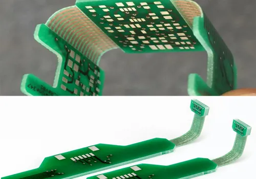
What Are Semi-Flex PCBs and Why Does Conversion Matter?
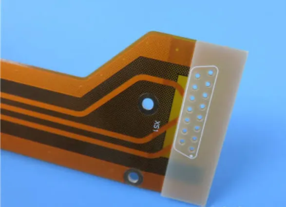
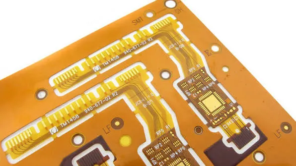
Semi-flex PCBs integrate rigid sections with localized flexible areas on a single board, unlike fully rigid or pure flexible circuits. These boards start as rigid FR-4 based structures, but specific regions are machined to reduce thickness, enabling controlled bending. This hybrid nature supports three-dimensional assembly, reducing connectors and wiring harnesses that add failure points. Conversion from rigid to semi-flex becomes essential in space-constrained products where boards must conform to enclosures or withstand vibration. Industry relevance grows in sectors demanding lightweight, reliable interconnects without the premium cost of full rigid-flex. Ultimately, semi-flex solutions improve signal integrity and mechanical durability in real-world deployments.
The decision to pursue semi-flex PCB conversion hinges on application requirements like bend radius and cycle life. Rigid boards excel in flat, stable setups, but they warp or crack under flexure. Semi-flex designs mitigate these issues by localizing flexibility, preserving component mounting areas. Engineers benefit from shorter assembly times and fewer parts, streamlining production. As devices shrink, this conversion trend supports miniaturization while adhering to reliability benchmarks.
Technical Principles Behind Semi-Flex PCBs
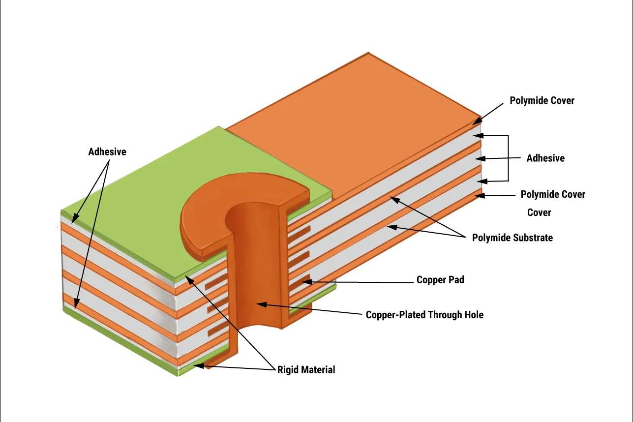
Semi-flex PCBs rely on controlled depth milling or etching to create flex zones, typically thinning the core to 0.1 to 0.2 mm while keeping rigid areas at standard thicknesses. Copper layers in flex regions are limited to one or two for optimal bend performance, preventing cracking during repeated flexure. The dielectric in these areas uses thin FR-4 or compatible films, ensuring adhesion and insulation under strain. Bend mechanics follow principles where radius relates to material thickness and width, guiding layout to avoid stress concentrations. Thermal expansion differences between rigid and flex zones require balanced stackups to minimize delamination risks.
Material selection emphasizes compatibility, with coverlays or films protecting traces in bend areas. Fabrication starts with rigid multilayer lamination, followed by precise routing to expose flex sections. Solder mask application varies by zone, thinner in flex areas to reduce stiffness. Electrical performance remains comparable to rigid boards, with controlled impedance in traces. Mechanical testing verifies cycle endurance, ensuring designs withstand installation bends without fatigue.
IPC-6013 provides qualification criteria for such hybrid boards, specifying visual and electrical inspections post-flexure. Adhering to these ensures consistency across prototypes and production.
Key Semi-Flex PCB Design Considerations
Semi-flex PCB design considerations begin with defining flex zones based on mechanical needs, such as connector tails or interconnects between modules. Trace routing in these areas must incorporate wider widths and curved paths to distribute stress evenly, avoiding 90-degree bends that initiate cracks. Stackup planning differentiates rigid and flex sections, with thinner cores and reduced via densities in bendable regions. Component placement prioritizes rigid areas for heavy parts, while flex zones host signals or passives tolerant of movement. Signal integrity analysis accounts for microstrip changes due to thinning, potentially requiring length matching adjustments.
Thermal management poses challenges, as flex areas have lower heat dissipation than rigid sections. Ventilation or heat sinks on rigid parts help, but simulations predict hotspots. Environmental factors like humidity influence flex durability, necessitating conformal coatings selective to zones. Minimum bend radius, often several times the flex thickness, dictates enclosure fit. Fabrication tolerances tighten for milling depths, impacting yield if not specified clearly.
Compliance with IPC-2223 guidelines for flex-to-install applications ensures designs suit one-time or limited-cycle bends. These standards outline bend allowances and material qualifications.
Best Practices and Tips for Semi-Flex PCB Conversion
Semi-flex PCB design tips start with auditing existing rigid designs to identify flex candidates, like areas prone to warpage or needing 3D folding. Begin conversion by exporting schematics and duplicating layouts in design tools, then segmenting stackups per zone. Prototype iterations test bend feasibility, using fixtures to simulate assembly stresses. Collaborate with fabricators early for depth milling capabilities, specifying tolerances like ±0.05 mm. Documentation includes bend direction, radius, and cycles, preventing misinterpretation.
Optimize traces with teardrops at pads in flex areas for strain relief, and use ground planes judiciously to avoid stiffening. Simulate mechanical flexure via FEA tools integrated in design flows, predicting failure modes. For high-density interconnects, limit vias in flex zones to blind or filled types. Assembly sequencing places flex bends last, reducing handling damage. Post-conversion validation includes continuity checks after bending.
Essential Semi-Flex PCB Design Tools and Software
Semi-flex PCB design software must handle multi-zone stackups, allowing custom core thicknesses and layer transitions. Features like dynamic routing for curved traces and 3D visualization aid bend previews. Integrated simulators assess strain and impedance shifts during flex. General-purpose tools support rigid-flex extensions, enabling semi-flex via user-defined profiles. Stackup editors calculate effective flex properties, crucial for conversion accuracy.
Mechanical CAD import verifies enclosure compatibility, overlaying bent PCB models. DRC rulesets customize for semi-flex, flagging sharp bends or thin dielectrics. Gerber output includes separate panels for rigid and flex processing. Version control tracks conversion changes, facilitating iterations. Training on these tools accelerates adoption, with tutorials focusing on hybrid workflows.
Challenges and Troubleshooting in Semi-Flex Conversion
Common hurdles in semi-flex PCB conversion include delamination at rigid-flex interfaces from mismatched CTEs. Mitigate by gradual thickness transitions and adhesive fillers. Cracking in milled areas stems from over-flexing; enforce radius limits via design rules. Yield drops if milling precision falters, so specify step-down routing. Signal crosstalk rises in thinned dielectrics, addressed by shielding planes.
Assembly defects like tombstoning occur if flex warps components; use jigs for flat soldering. Testing reveals intermittent opens post-bend, traced to trace fatigue. IPC-A-600 outlines acceptability criteria for such boards, aiding inspections. Troubleshooting logs correlate failures to design tweaks, refining future conversions.
Conclusion
Semi-flex PCB conversion transforms rigid designs into versatile hybrids, ideal for modern compact electronics. Key principles like zoned stackups and stress-aware routing ensure reliability. Design considerations and tips guide engineers through challenges, leveraging standards for quality. Tools streamline the process, from simulation to fabrication handoff. Embracing this shift yields space savings, fewer connectors, and enhanced durability. Future designs will increasingly adopt semi-flex for dynamic applications.
FAQs
Q1: What are the main steps in semi-flex PCB conversion from a rigid design?
A1: Semi-flex PCB conversion starts with analyzing the rigid layout for flex zones, then adjusting stackups to thin cores in those areas. Route traces with curves and wider paths, simulate bends for stress, and prototype with precise milling specs. Validate through cycle testing to confirm integrity. This logical progression minimizes risks and optimizes performance for electric engineers.
Q2: How do semi-flex PCB design considerations differ from rigid boards?
A2: Semi-flex PCB design considerations emphasize bend radii, trace strain relief, and zoned materials, unlike uniform rigid stackups. Limit flex layers to 1-2, avoid vias in bends, and balance CTEs at transitions. Thermal and mechanical simulations are critical. These factors ensure durability in flexed states without compromising rigid support.
Q3: What features should semi-flex PCB design software include?
A3: Semi-flex PCB design software needs multi-zone stackup editors, 3D bend previews, and DRC for flex rules. Integrated FEA for strain analysis and curved routing tools support conversion. Impedance calculators adapt to thinning, aiding signal integrity. Such capabilities enable seamless rigid-to-semi-flex transitions.
Q4: What are essential semi-flex PCB design tips for reliability?
A4: Semi-flex PCB design tips include teardrops at pads, gradual thickness ramps, and selective coatings. Prototype bends early, specify milling depths tightly, and test cycles per application. Ground fills in rigid areas stabilize, while flex zones prioritize signals. These practices enhance long-term performance.
References
IPC-6013D - Qualification and Performance Specification for Flexible and Rigid-Flex Printed Boards. IPC, 2014
IPC-2223C - Section Qualification and Performance of Permanent Polymer Thick Film Printed Board. IPC, 2019
IPC-A-600K - Acceptability of Printed Boards. IPC, 2020