Overview
In electronic devices, the power module is a core component that converts an input DC voltage into the various DC voltages required by the system. DC-DC converters, especially switching converters, are widely used because of their efficiency, compact size, and light weight. Designing a robust DC-DC converter requires careful attention to layout, electromagnetic compatibility, current handling, and thermal management.
Placement and General Considerations
To optimize power delivery, switching power supplies should be placed close to the target IC to avoid long output traces that cause voltage drop. To reduce electromagnetic interference, avoid placing sensitive components near the switching converter. For improved stability and reliability, consider wiring strategy, reinforced ground connections, and thermal ground design.
01. DC-DC Application Types
DC-DC supplies are the core devices for DC voltage conversion and regulation, including LDO regulators and switching DC-DC converters. Switching converters offer low power loss, high efficiency, small size, and good robustness across a wide output range, so they are widely used in electronic systems.
02. Operating Principle
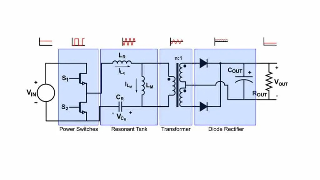
The operating principle of a DC-DC converter involves voltage conversion and regulation, primarily implemented by a switching converter. The converter transforms the input DC voltage into the required output DC voltage. The process can be divided into three main steps:
- Filtering: After the input is rectified to pulsating DC, filter circuits remove ripple to produce smooth DC for the converter.
- Conversion: The DC-DC converter uses power switches and energy-storage inductors to produce pulsed power. Pulse transformers, rectifiers, and filter circuits then generate the output voltage. Conversion is controlled by PWM (pulse-width modulation) or PFM (frequency modulation) adjusting the switch timing. Switching actions occur very quickly, typically in microseconds, much faster than adjustments in linear regulators.
- Regulation: Output voltage stability is achieved via a feedback loop. When the output voltage rises, the sampled feedback signal increases; the comparator produces a larger error signal, which reduces the switch duty cycle via PWM or PFM control, lowering the converter's average output power and stabilizing the output voltage.
03. Key Component Selection
1. Output Inductor
Inductors store magnetic energy and help ensure stable current output. Choosing an inductor requires balancing size: larger inductance reduces losses but slows response; smaller inductance improves transient response but increases losses. Consider saturation current to ensure effective filtering.
2. Divider Resistors
Voltage divider resistors form the feedback network that reports the output voltage to the control circuit, enabling precise control of the PWM duty cycle and stable output. Use high-precision resistors to maintain accuracy.
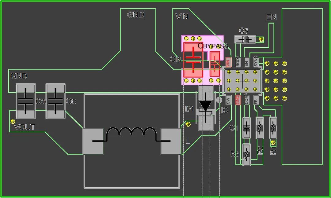
3. Input Capacitors
Select input capacitors with regard to equivalent series inductance and self-resonant frequency. Large-value capacitors filter low-frequency noise, while small-value capacitors filter high-frequency noise. Parallel combinations often yield better overall filtering and a stable input voltage.
4. Output Capacitors
Output capacitors reduce switching ripple and ensure a clean output current. Larger capacitance generally lowers impedance and makes it easier for ripple current to flow. Choosing appropriate output capacitance and ESR is critical to minimize ripple and ensure stable operation.
When selecting these components, balance multiple factors to achieve the optimal tradeoffs: inductor selection balances efficiency and response speed; divider resistors must provide stable, accurate feedback; input and output capacitors should be chosen for the noise characteristics at the operating frequencies; output capacitors require consideration of capacitance and ESR to minimize ripple.
04. PCB Layout and Routing Recommendations
Obtain the chip datasheet and follow the recommended layout and routing guidelines when designing the power module.
1. Layout Guidelines
- Place the power supply close to the IC it powers to avoid long low-voltage output traces and minimize voltage drop.
- Avoid placing sensitive components near the switching converter to reduce EMI impact.
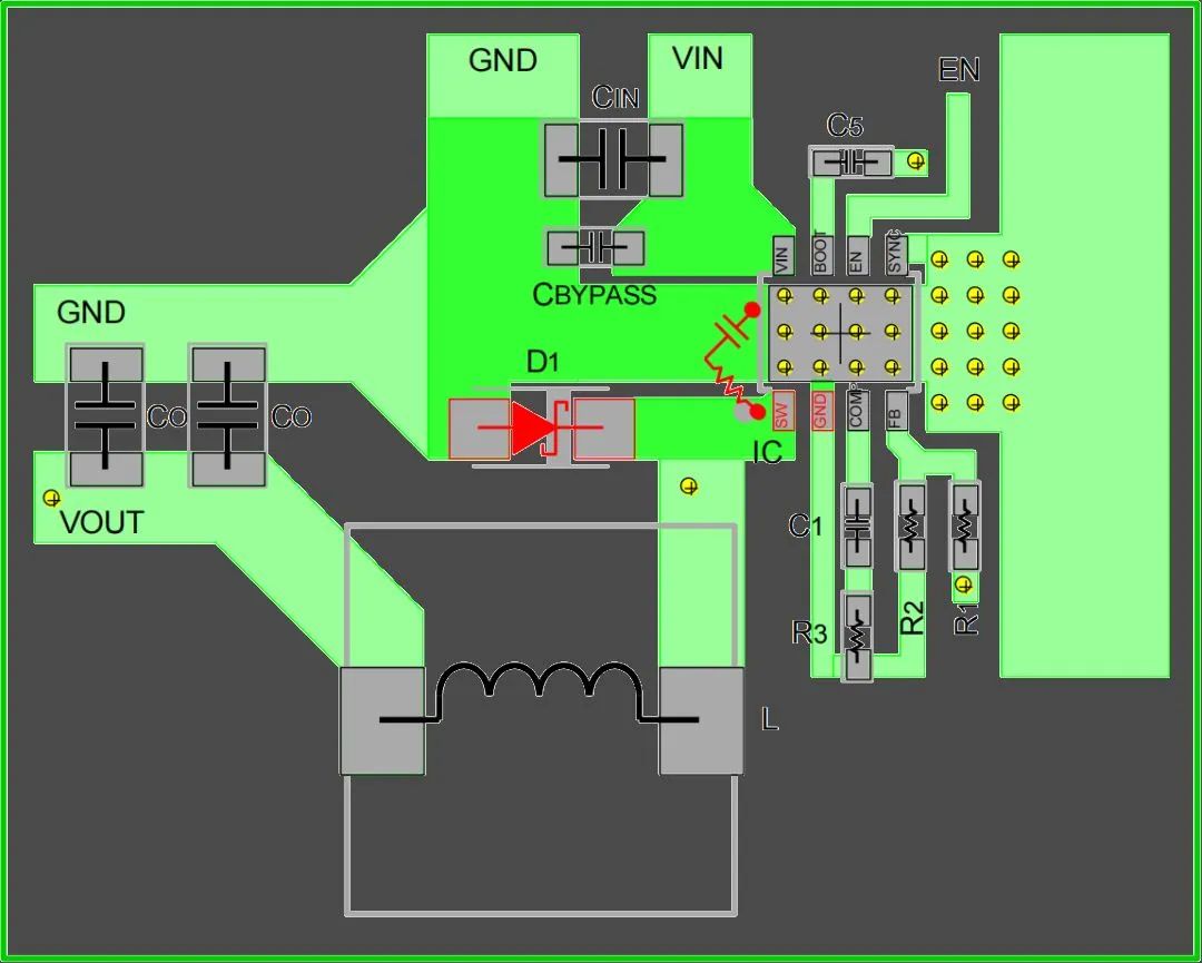
- Organize the layout around the power chip. Ensure adequate spacing between the filter's input and output to prevent noise coupling from input to output. Place components neatly and compactly on the PCB to shorten interconnections and leads.
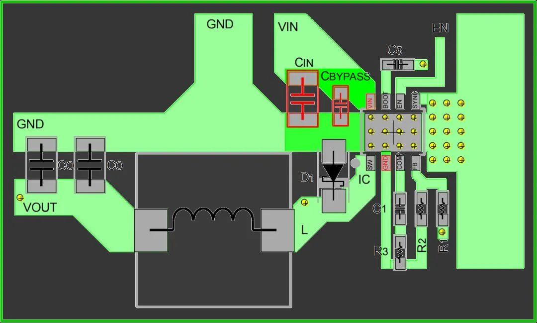
2. Routing Guidelines
- Avoid parallel traces for input and output to reduce unnecessary electromagnetic coupling.
- Widen ground traces between input and output to ensure stable current flow and reduce feedback coupling.
- Heavy-current traces, such as common ground and power input/output traces, should be as wide as possible to reduce trace resistance and voltage drop, and to minimize parasitic coupling that can cause oscillation.
3. Thermal Considerations
- Provide ample copper area for thermal dissipation, as switching converters can generate significant heat.
- Use large copper pours and multiple vias on input and output areas to meet current requirements and improve heat dissipation.
05. Conclusion
DC-DC converters play a critical role in electronic systems. Their design involves multiple precise and interdependent aspects. From understanding operating principles to carefully selecting key components and optimizing layout and routing, each step requires solid technical knowledge and methodical engineering. These considerations help achieve efficient, stable, and reliable converter designs.