Introduction
In modern electronics design, power integrity is an essential aspect of printed circuit board design. To ensure stable device performance, designers must consider the entire power path from the source to the load. Key elements include power modules, internal planes, and power-supply ICs. This article discusses three critical areas and provides practical guidance for PCB design.
Power Module Placement and Routing
As fundamental building blocks in the New energy industry, power modules are the energy source for electronic systems, and their performance, placement, and routing directly affect system stability and efficiency. Proper layout and routing reduce noise, ensure smooth current flow, and improve overall performance.
1. Power Module Placement
- Source handling: As the origin of the power path, the power module should be placed in a relatively clean environment to minimize noise coupling and avoid proximity to high-frequency or noise-sensitive components.
- Close to the load: Place the power module as close as possible to the powered ICs to reduce transmission losses and minimize the area required on internal planes.
- Thermal considerations: Ensure there are no obstructions above the power module to allow heat dissipation. If necessary, add heatsinks or active cooling.
- Avoid loops: Route traces to avoid forming current loops, which can increase electromagnetic interference.
2. Power Module Routing
- Width and current: Choose trace widths based on the required current. Higher currents require wider traces to maintain current-carrying capacity.
- Via count: When routing power between layers, provide enough vias to handle the current and avoid via overheating.
- Separation and coupling: Maintain appropriate spacing between power traces and other signal traces to avoid undesired coupling.
- Return path: Keep ground return paths continuous and avoid abrupt narrowings or breaks in ground traces.
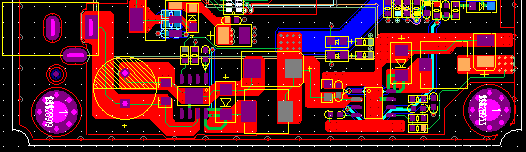
Internal Plane Design and Planning
1. Stackup Design
In EMC-aware PCB design, stackup planning is critical. Consider routing and power partitioning when defining layer stackups.
- To ensure low impedance and effective coupling between power and ground planes, the separation between power and ground planes should be no greater than 10 mil. A separation under 5 mil is preferred where manufacturable.
- If a single continuous power plane is not feasible, routing a power plane on a signal layer with adjacent power and ground planes can form a plane capacitor with minimal AC impedance, improving high-frequency performance.
- Avoid placing two power planes with large voltage differences too close to each other to prevent noise coupling; increase spacing where possible.
- Reference planes, especially power reference planes, should maintain low impedance. Optimize using bypass capacitors and stackup adjustments.
Related Reading: Implementing Power Integrity Analysis for Efficient ECU PCB Design
2. Partitioning Multiple Power Nets
- For small, localized power nets such as an IC core voltage, consider copper pours on signal layers to preserve the integrity of dedicated power planes while minimizing radiated noise from surface copper.
- Choose partition widths appropriately: for voltages above 12V consider 20–30 mil; for lower voltages 12–20 mil. Increase widths where analog and digital power domains are separated to reduce digital-to-analog noise coupling.
- Simple power routing should be completed in routing layers; longer power runs should include filtering capacitors.
- Maintain regular shapes for partitioned power planes. Avoid irregular shapes, thin fingers, or dumbbell-shaped partitions that can create resonance and increase power impedance.
3. Plane Filtering
- Power planes should be closely coupled to ground planes.
- For devices operating above 500 MHz, rely primarily on plane-level capacitance for filtering and use combined capacitor networks. Validate filtering effectiveness with power integrity simulation.
- Control the mounting inductance of decoupling capacitors by widening capacitor lands and increasing via sizes or counts to ensure the power-ground impedance meets target levels.
Power-Supply IC Placement and Routing
Power-supply ICs are central to device power delivery. Ensuring power integrity around these ICs is key to performance and stability.
1. Routing for Power Pins
To provide stable current delivery, widen traces connected to power pins. Trace widths should match or exceed the width of the IC pins. Minimum widths should not be less than 8 mil, and 10 mil is recommended where possible. Wider traces reduce impedance, lower power noise, and ensure adequate current to the IC.
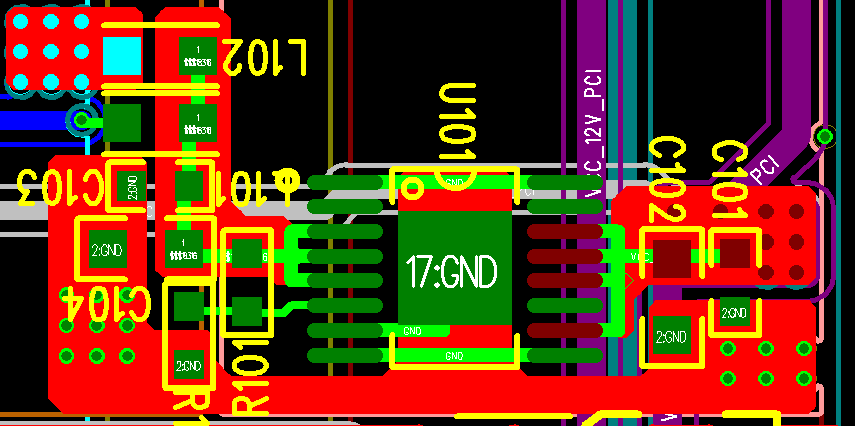
2. Decoupling Capacitor Placement and Routing
Decoupling capacitors play a critical role in power integrity. Typically use a combination of large and small capacitors:
- Large capacitors: Distribute larger capacitors around the IC to filter low-frequency noise and provide bulk charge due to their lower resonant frequencies and larger effective radius.
- Small capacitors: Place small-value capacitors as close as possible to IC power pins to filter high-frequency noise. If placed too far, they may not be effective.
3. Routing Multiple Parallel Decoupling Capacitors
Parallel multiple decoupling capacitors to reduce the equivalent series inductance (ESL). When placing vias for these capacitors, stagger the power and ground vias to reduce mutual inductance between capacitors. This helps ensure that the combined ESL scales roughly as 1/N and improves overall filtering effectiveness and power stability.
Practical Considerations
In practice, consider current levels, trace widths, via counts, and coupling effects when choosing layout and routing strategies. Follow design rules and best practices to control and optimize power integrity. Use power integrity simulations and validation to confirm design choices before production.