Question
Why is a capacitor C1 commonly connected in a step-down (buck) converter?
Role of C1
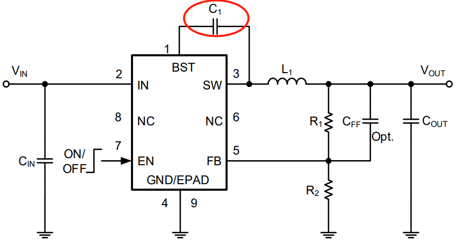
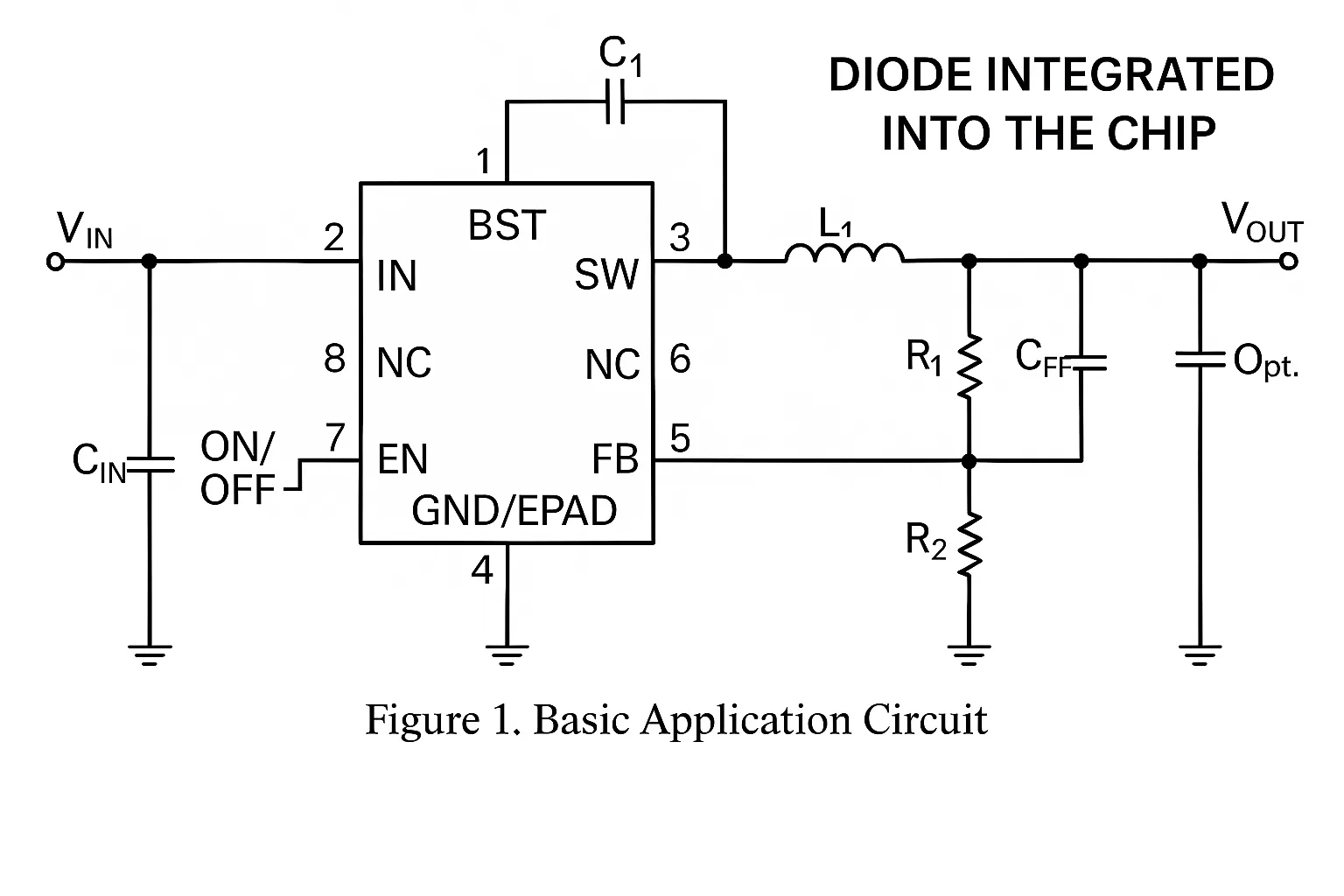
The bootstrap capacitor connected between SW (switch node) and BST provides a floating supply for the high-side driver. It stores charge so the high-side MOSFET gate driver has the required drive energy or power when the high-side switch needs to be turned on.
Conceptual background
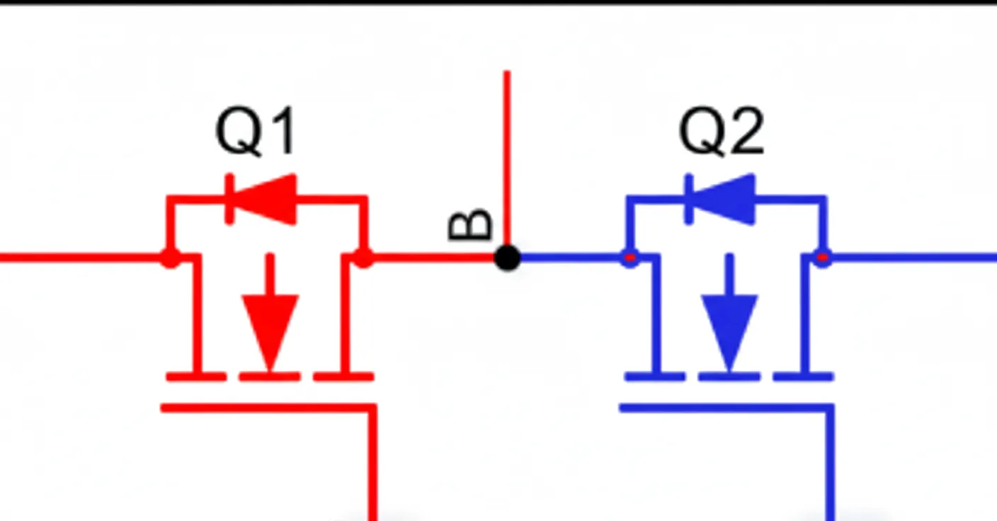
(1) Half-bridge structure: If Q1 is the high-side transistor, Q2 is the low-side transistor. This half-bridge arrangement is common in power supplies.
(2) Synchronous rectification in a buck converter
High Side (HS): the switch node connected to the input positive rail; typically refers to the upper transistor.
Low Side (LS): the switch node connected to the reference ground; typically refers to the lower transistor.
Below is a buck converter using synchronous rectification, where the freewheeling diode is replaced by an active device (enhancement MOSFET Q2) to reduce conduction losses.
(3) Driving the half-bridge
In a single-reference supply system, the high-side device reference (its source) is floating, while the low-side device is referenced to system ground. The challenge is how to drive the high-side gate using a supply that shares the system reference, since no fixed return to ground exists when the low-side transistor is off.
The source of Q1 swings between the input voltage VB and ground. Q1 and Q2 operate complementarily; they must not be on at the same time to avoid shoot-through.
Typically, VDD powers the controller and is derived from the input VB through a regulator. When Q2 is off and Q1 must be turned on, using the ground-referenced VDD to charge Q1's gate is not feasible because VDD is lower than VB and, with Q2 off, there is no conduction path to form the gate charge circuit.
Bootstrap floating supply
The bootstrap network between SW and BST creates a floating supply for the high-side driver so the driver can turn on the high-side transistor when needed.
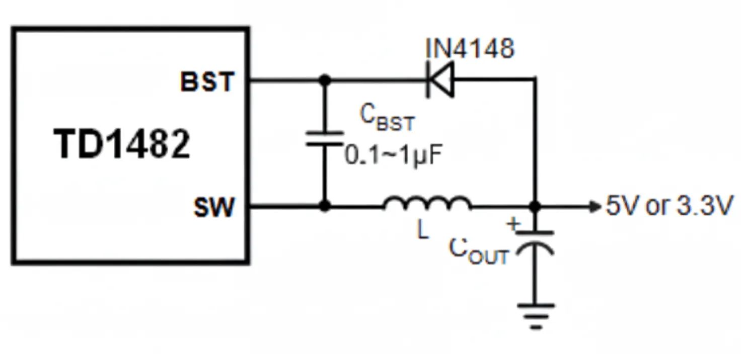
1. Bootstrap circuit components: diode D1 and capacitor C1.
2. Bootstrap charging operation
Q1 and Q2 operate complementarily. When the low-side transistor Q2 is on, VDD charges C1 through diode D1, returning to ground via Q2 to complete the charging path.
3. Bootstrap as floating supply for high-side gate drive
With Q2 off, C1 holds the stored charge and forms an independent supply. When Q1 needs to be turned on, the bootstrap capacitor supplies the driver so Q1's gate can be driven.
Practical driver implementations
Common solutions include half-bridge driver ICs or buck power-management ICs that implement a bootstrap high-side driver.
(1) Half-bridge driver IC example: the CBOOT pin is the bootstrap storage capacitor.
(2) Buck PMICs with synchronous rectification often integrate the bootstrap diode; only the bootstrap capacitor is required externally.
Choosing C1 value and failure modes
For low-power DC-DC converters, vendors usually recommend a bootstrap capacitance. The value is calculated based on driver power or the MOSFET gate charge requirements.
However, bootstrap can fail to supply the high-side transistor in some cases. If the low-side on-time is very short or the gate-drive power requirement is high, the bootstrap capacitor may not charge sufficiently before it is needed, or it may not hold enough charge to meet the drive energy demand. When bootstrap cannot meet the high-side supply needs, an alternative is to use an isolated secondary supply or a separate reference to provide the high-side driver power, for example via a transformer or separate winding.