Introduction
Antenna is a critical component for devices that use wireless communication. Routers, computers, smartphones, Bluetooth headsets, mice, and keyboards all rely on antennas. When selecting an antenna, performance and cost must be balanced. This article summarizes common antenna types and key PCB design considerations.
Common Antenna Types
1. PCB Onboard Antennas
PCB onboard antennas have low cost but generally lower performance. Several common forms exist.
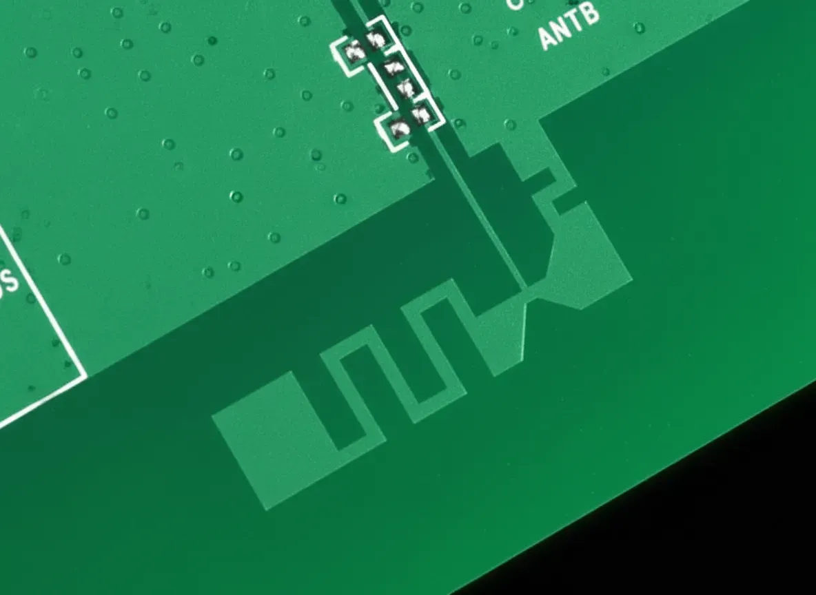
a. Planar Inverted-F Antenna (PIFA)
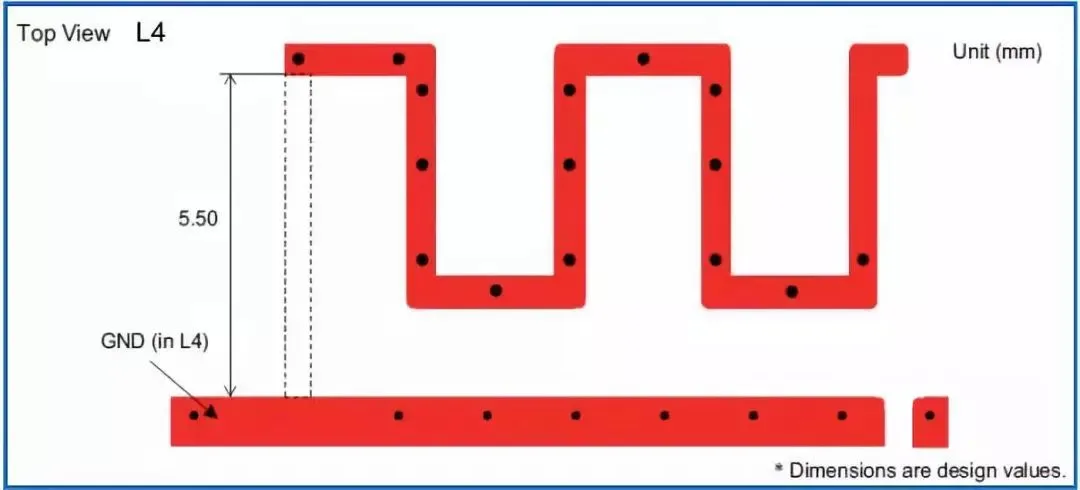
The planar inverted-F antenna (PIFA) is widely used on PCBs. Examples are shown below.
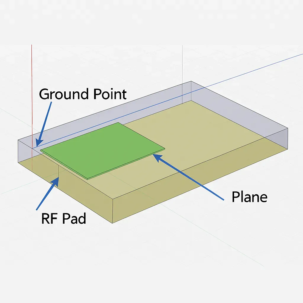
When designing an inverted-F PCB antenna, follow RF design principles: copper traces and conductors behave as distributed RLC networks at RF, so connections that look like shorts at DC may not be shorts at RF. Key PCB points for inverted-F antennas:
- Use validated antenna layout libraries when available. If space is constrained, perform electromagnetic simulation to create a custom antenna.
- The RF feed trace must be 50 ohm impedance.
- The ground connection for the feed must be solid.
- The ground plane should include multiple ground vias near the antenna; via spacing should follow layout guidelines for the chosen design.
- All copper layers under the antenna region must be cleared (no copper).
- Place the antenna at a PCB corner when possible, with at least three sides free of surrounding metal or ground; this improves performance.
Mobile devices typically use a planar implementation of the inverted-F structure, where a planar radiator, a ground connection, and an RF feed form the inverted-F. Planar PIFA in phones performs better than simple PCB trace antennas while keeping low cost and small form factor.
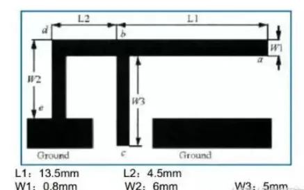
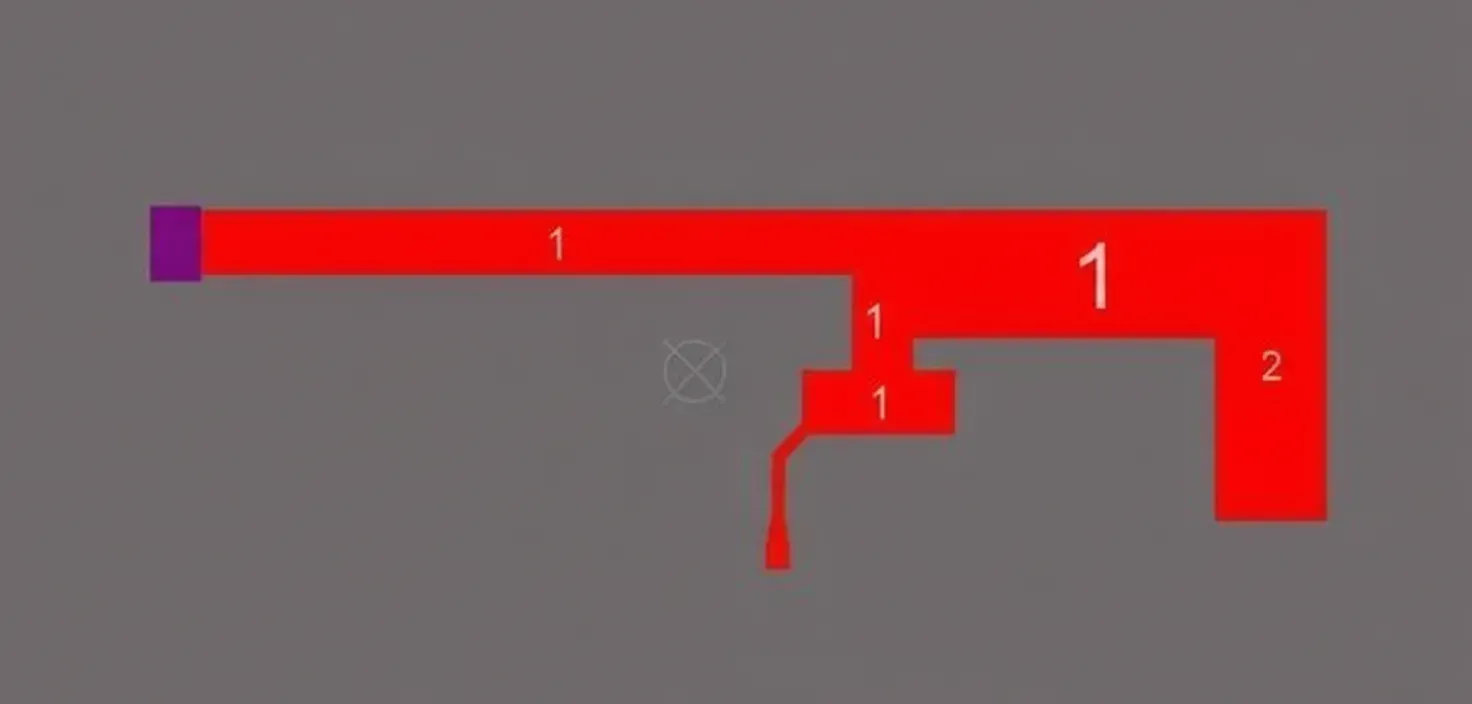
b. Inverted-L PCB Antenna
The inverted-L PCB antenna is another common PCB trace type. Examples are shown below; variants are often used to fit limited space and tune the operating frequency.
The inverted-L requires similar PCB layout rules as the inverted-F. In general, inverted-F antennas offer somewhat better tuning ability because of the grounded feed point.
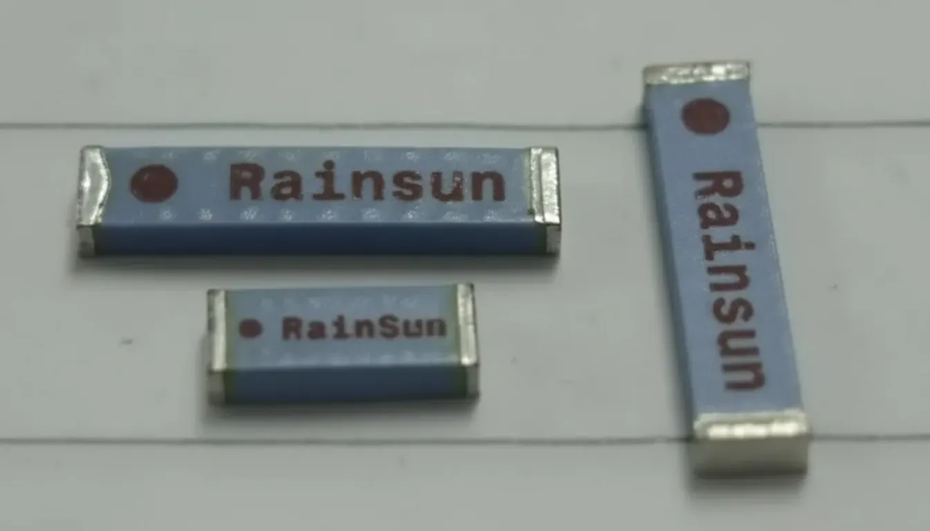
2. Ceramic Patch Antennas
Ceramic patch antennas are packaged as discrete components. One side connects to RF and the other to ground. The ceramic element converts the high-frequency near field between the radiator electrode and ground into radiated electromagnetic waves.
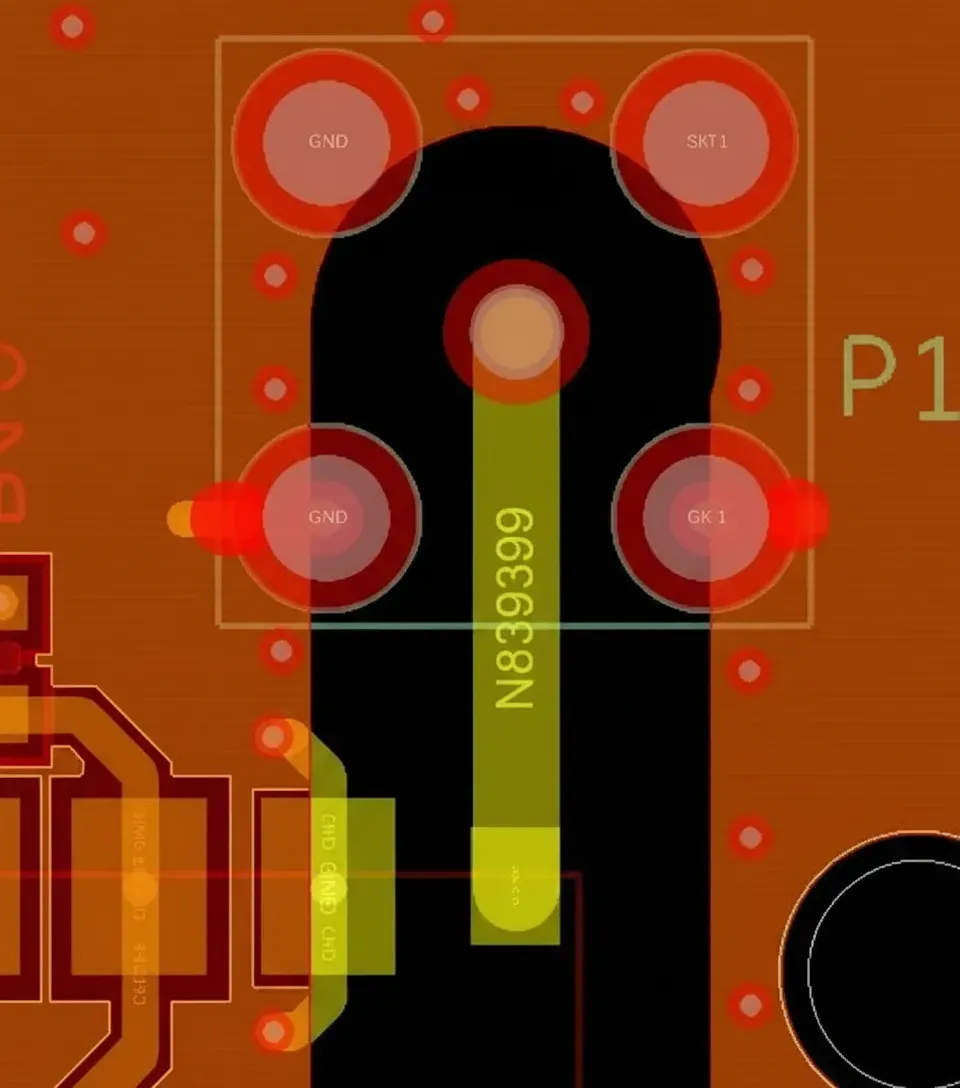
Recommended PCB placement: place the ceramic patch at the board edge, with one pad to ground and one to RF signal. Keep all PCB layers under the antenna cleared (no copper) in the antenna clearance region. Ensure ground copper is connected with multiple ground vias.
3. Whip (Rod) Antennas
Rod antennas provide the best radiation when placed in free space, offering superior range, but they are larger, costlier, and typically must protrude outside the enclosure.
PCB design considerations for rod antennas:
- If the RF feed stub is short, clear all layers under the RF feed trace. If the feed trace is long, control its characteristic impedance. On a multilayer board, keep the layer immediately below the feed clear and use the next reference layer to control impedance; target 50 ohm for the feed.
- Ensure nearby ground copper is reliably connected with sufficient ground vias.
Bluetooth Antenna Design Notes
Inverted-F Antenna for Bluetooth
Inverted-F antennas can be wire- or planar-shaped. Using higher-dielectric insulating materials reduces antenna size. As a common onboard antenna, inverted-F designs balance cost and size and are often placed on the PCB top layer. Maintain an antenna clearance area with no ground copper around the antenna.
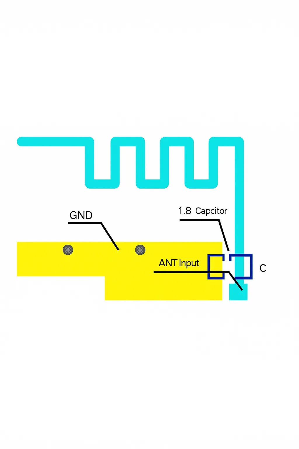
Meander (Folded) Antenna
Meandered antennas are longer than a simple quarter wavelength and their effective length depends on geometry and the board area they occupy. They are typically PCB-mounted. Like inverted-Fs, keep the antenna on the top layer and ensure a cleared area around it.
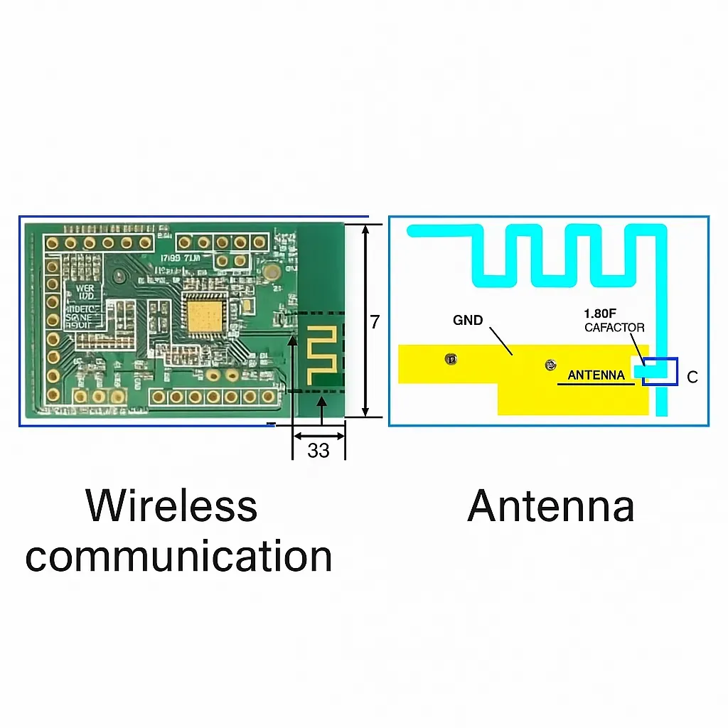
Note: antenna length calculation (meters): length = (300 / f) * 0.25 * 0.96, where f is frequency in MHz and 0.96 is the wavelength shortening factor. For Bluetooth at 2.4 GHz, this yields approximately 31 mm.
Ceramic Antenna for Bluetooth
Ceramic antennas are suitable for compact Bluetooth devices and are available as block or multilayer types. Because ceramic has higher dielectric constant than typical PCB materials, ceramic antennas are much smaller. Ceramic dielectric loss can also be lower, making them suitable for low-power Bluetooth modules. Keep the PCB area around the ceramic antenna clear of copper.
2.4 GHz Rod Antenna for Bluetooth
2.4 GHz rod antennas are larger but provide longer range. PCB layout rules are similar: maintain a cleared area around the antenna.
Other Bluetooth Antenna Guidelines
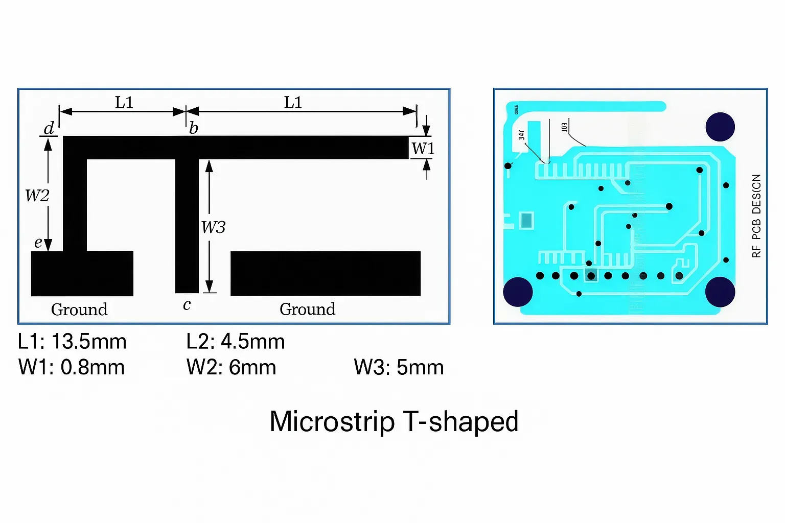
- RF signals above about 400 MHz are susceptible to attenuation by nearby ground. Maintain a clearance between the antenna signal and nearby ground at least three times the trace width.
- Characteristic impedance of microstrip and stripline traces depends on stack-up thickness, trace width, vias, and dielectric constant.
- Vias introduce parasitic inductance that can attenuate high-frequency signals. Avoid vias on RF traces when possible.
Internal Phone Antennas
Modern smartphones use internal antennas primarily in two categories: PIFA and monopole. Properly designed PIFA offers good electrical performance and specific absorption rate (SAR) characteristics, making it a common choice for internal antennas. Monopole designs can also achieve high performance but may have higher SAR and are less suitable for foldable or sliding mechanisms.
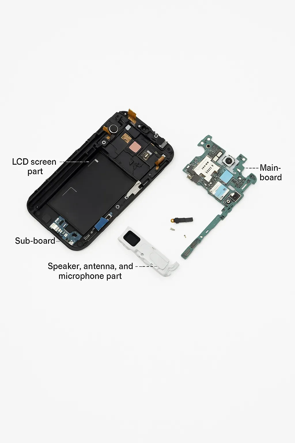
Examples of internal antenna placements in several phones:
Galaxy Note 2: the white module at the bottom is the antenna module.
Galaxy S5: various RF modules and antenna switching components are integrated; different colored regions indicate antenna switch and RF transceiver/receiver components.
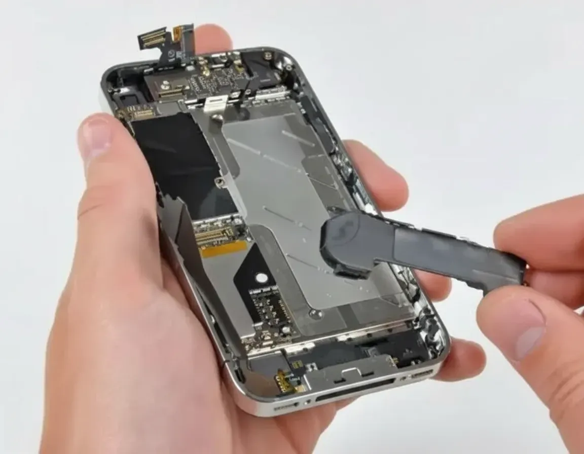
iPhone 4S: the antenna is placed at the bottom and the phone also uses an external metal antenna element.
iPhone 6: antenna elements were moved to the upper area, integrated with metal frame design.
Antenna Technology Evolution and MIMO
Early mobile phones used external low-frequency analog antennas. As mobile technology evolved, internal antennas made from stamped thin metal or flexible FPC became common due to space and cost advantages. Later, laser-direct-structuring (LDS) techniques allowed antennas to be formed directly on specially treated plastic moldings, which is common in mid- to high-end devices.
MIMO (Multi-input Multi-output) uses multiple transmit and receive antennas to increase throughput and range without increasing bandwidth or total transmitted power. MIMO leverages spatial degrees of freedom provided by multiple antennas to improve spectral efficiency and link reliability. Commonly expressed as A×B MIMO, e.g., 2×2 MIMO uses two transmit and two receive antennas and can roughly double capacity compared to SISO.
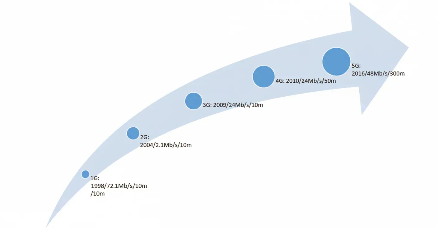
5G and Antenna Trends
Antennas remain essential for wireless devices. Antenna length correlates strongly with wavelength, commonly at quarter- or half-wavelength dimensions. For example, a 900 MHz band requires antenna lengths on the order of several centimeters.
Sub-6 GHz 5G frequency bands overlap with existing 4G bands, so antenna element sizes for Sub-6 GHz devices remain centimeter-scale. To meet higher throughput requirements, 5G devices use more antenna elements via MIMO. Increasing antenna count requires careful rearrangement of element shapes and placement, impacting rear cover design and routing. Some devices integrate a large number of antenna elements; for example, a flagship device may integrate dozens of antennas, including multiple 5G elements.
References and Further Reading
This article summarized antenna types and practical PCB layout considerations for designers of wireless devices. Key topics include PIFA, inverted-L/F, meander, ceramic patch, rod antennas, MIMO, and Sub-6 GHz 5G trends.