(1) Modern chip integration
Chips are increasingly integrated, and it is common for a single package to include one or multiple RF systems.
In chip architectures, zero-IF or low-IF topologies are often used because they are simpler and do not require off-chip filters like superheterodyne receivers.
As shown below:
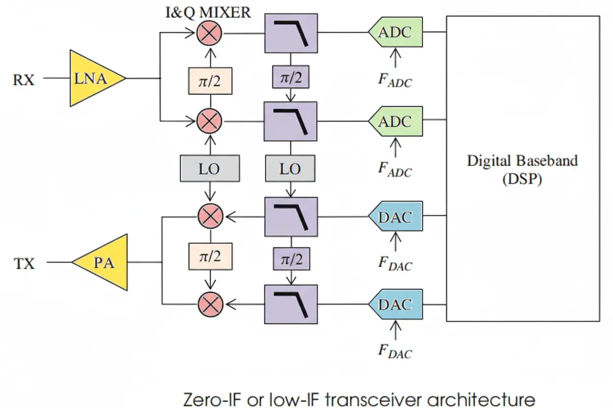
Although the RF front end can be simpler, the digital part must perform substantial calibration to compensate for nonidealities.
Which real-world component imperfections affect overall system performance?
Thermal noise and flicker noise
All physical devices exhibit random electron motion that produces random noise, i.e., thermal noise.
For example, a passive resistor R at temperature T Kelvin produces a noise voltage given by the usual relation:
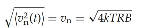
If the load resistance equals that resistor, the noise power delivered to the load is the familiar kTB expression. Without considering system bandwidth and at T = 290 K, the noise density is ?174 dBm/Hz.
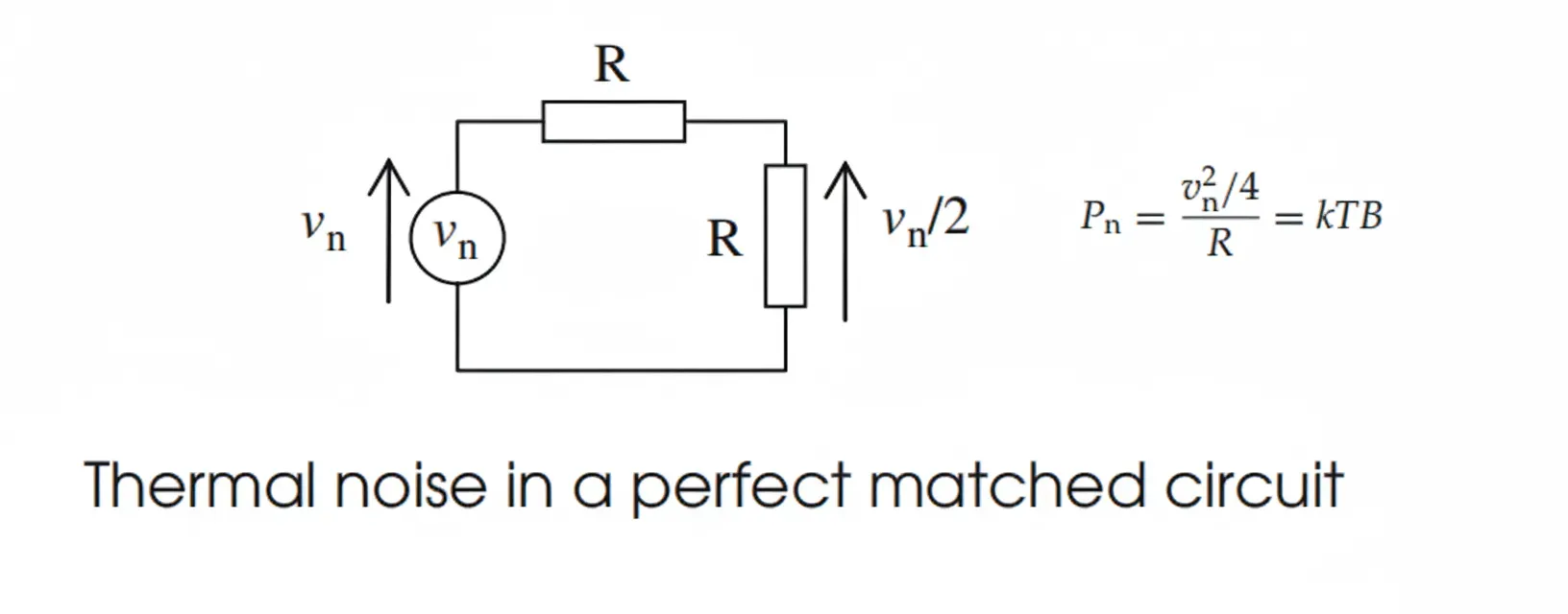
Active devices also exhibit flicker noise (1/f noise). Because flicker noise is concentrated near DC, it strongly affects zero-IF architectures and to a lesser degree low-IF architectures.
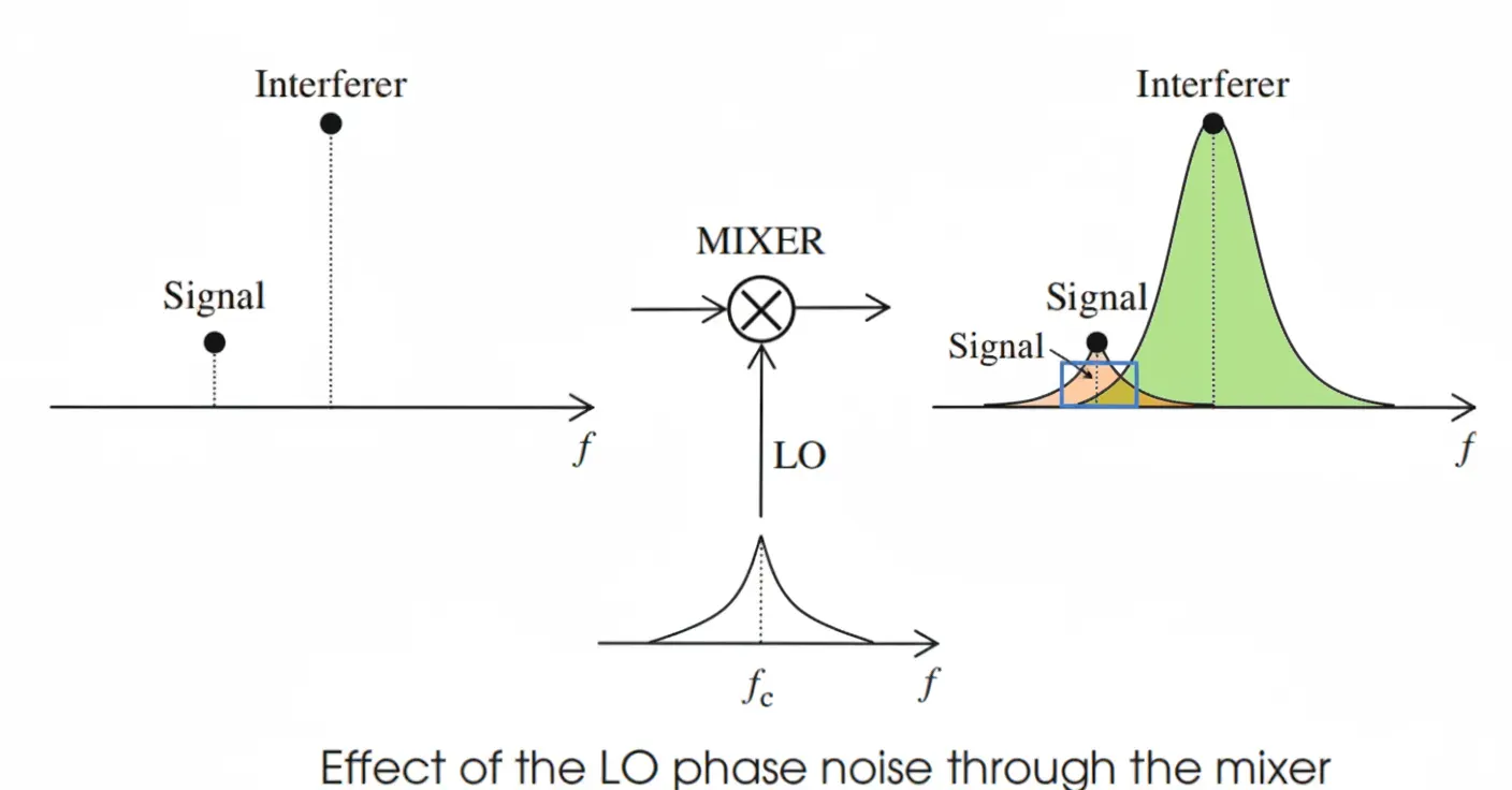
LO phase noise
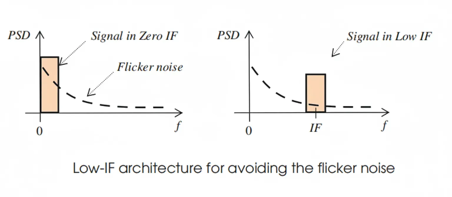
An ideal oscillator has a delta-function spectrum, but real oscillators exhibit phase noise skirts as shown below.
The local oscillator (LO) phase noise in transceivers affects the system in two main ways. First, multiplication of the signal by the LO phase-noise spectrum increases in-band noise. Second, phase-noise mixing of interfering signals with the LO can cause additional in-band noise through reciprocal mixing.
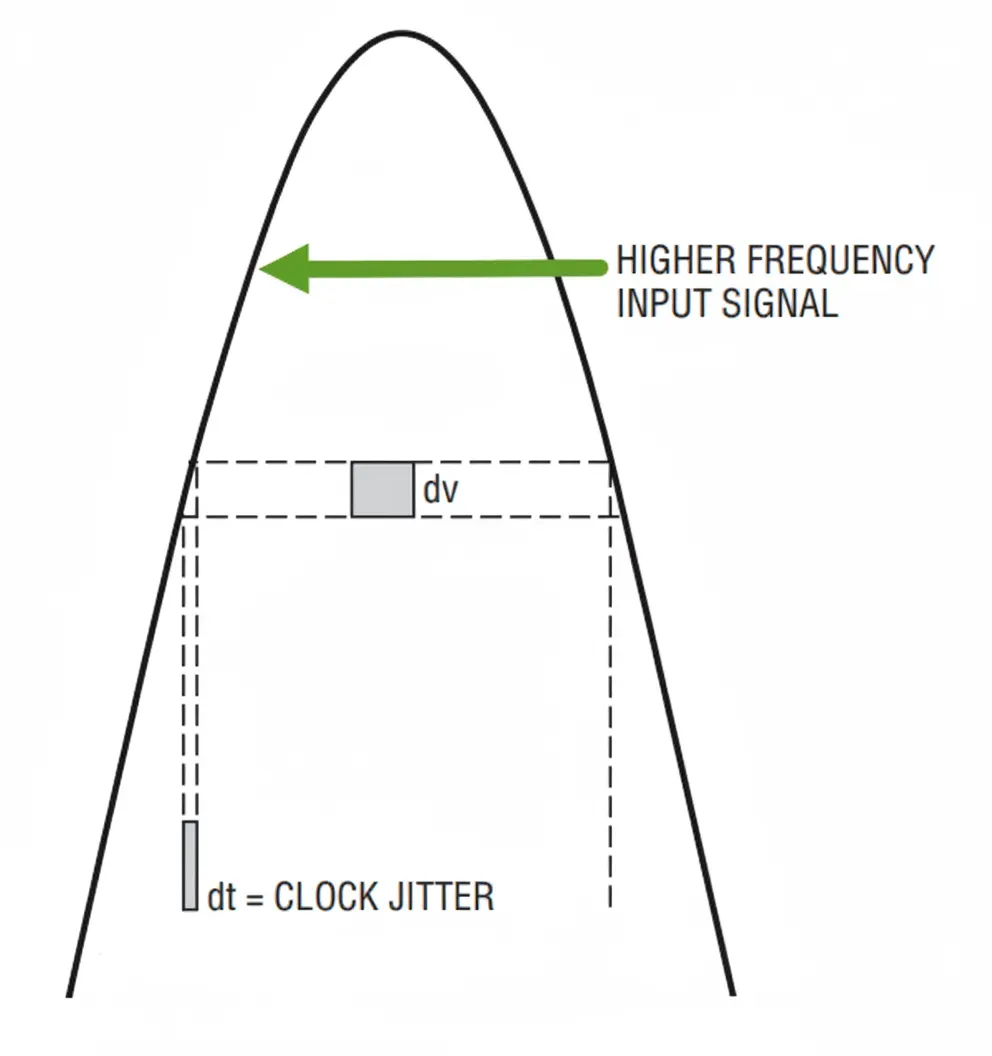
Sampling jitter
ADCs and DACs mark the boundary between analog and digital domains. Converting between domains requires a sampling clock.
The sampling clock is itself an oscillatory signal, and practical oscillators have phase noise, which in the time domain is seen as jitter.
Time-domain jitter causes sampling errors and therefore contributes noise to the conversion process.
Carrier frequency offset (CFO) and sampling frequency offset (SFO)
In communication systems, carrier frequencies are typically generated by phase-locked loops. Because the transmit and receive carrier frequencies can differ slightly, the downconverted signal at the receiver may contain a residual frequency error, known as carrier frequency offset (CFO).
Similarly, the ADC and DAC sampling clocks may differ slightly, producing a sampling frequency offset (SFO) that also degrades system performance.
ADC/DAC quantization noise and clipping
ADC and DAC conversions introduce quantization noise, which limits achievable SNR.
In receiver design, the analog front end typically provides enough gain so that the ADC's own noise is small compared with the front-end thermal noise and can be neglected.
Clipping or truncation in the ADC can limit the signal PAPR (peak-to-average power ratio), which degrades effective SNR.
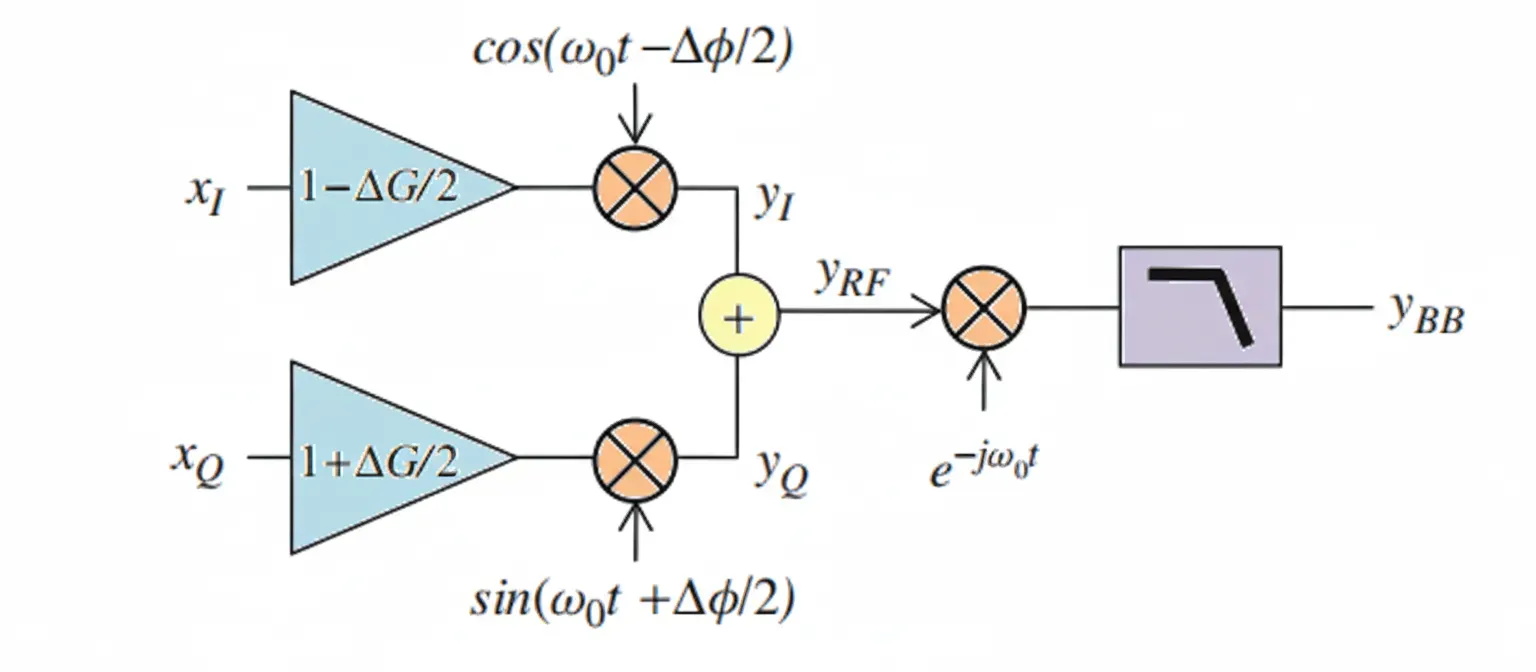
I/Q imbalance
Upconversion and downconversion use quadrature mixers. Practical I and Q paths can have gain and phase mismatches, which reduce SNR or generate unwanted out-of-band products.
Device nonlinearity
Receiver nonlinearity mainly affects large interfering signals and is characterized by intermodulation distortion and desensitization metrics.
Reference
[1] Lydi Smaini, RF Analog Impairments Modeling for Communication Systems Simulation: Application to OFDM-Based Transceivers