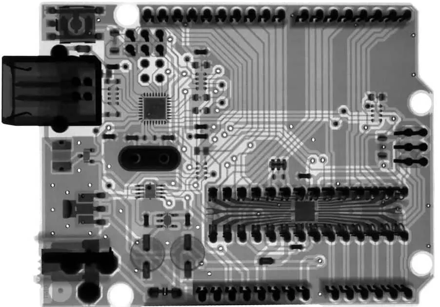
BGA Inspection
Ball Grid Array (BGA) components are essential in modern electronics, offering high-density interconnections for complex circuit boards. BGA Inspection refers to the specialized processes used to evaluate these packages for defects, ensuring reliability and performance in PCB assembly. Whether you are troubleshooting soldering issues, verifying component placement, or preventing failures in high-stakes applications like aerospace or consumer devices, understanding BGA Inspection techniques is crucial for maintaining quality standards. Common challenges in BGA Inspection include hidden solder joints that are not visible to the naked eye, making traditional visual checks insufficient. Professionals often rely on advanced methods such as X-ray imaging, which reveals voids, bridging, or misalignment beneath the package. Optical inspection tools, including automated optical inspection (AOI) systems, provide surface-level analysis, while endoscopic cameras offer detailed views of hard-to-reach areas. Best practices emphasize starting with non-destructive techniques to minimize rework costs, followed by thermal profiling to detect heat-related anomalies. For instance, implementing a step-by-step checklist—beginning with pre-reflow verification and progressing to post-assembly testing—can significantly reduce defect rates and improve yield in manufacturing environments. This tag gathers in-depth articles that delve into these inspection strategies, from beginner guides on basic tools to expert discussions on emerging technologies like 3D computed tomography. By exploring these resources, you can gain practical insights tailored to your specific needs, such as optimizing inspection workflows for prototyping or scaling up for production lines. Staying informed about BGA Inspection not only helps in diagnosing common problems like ball shear or pad cratering but also equips you with the knowledge to adopt preventive measures, ultimately enhancing the longevity and efficiency of your electronic designs.
Technical Articles

BGA Soldering Defects: A Comprehensive Guide for SMT Process Engineers

Dye Stain Analysis of SMT BGA Defects: A Review of Five Typical Cases
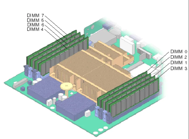
Why You Should Not Place Components Larger Than 3216 Directly Under a BGA
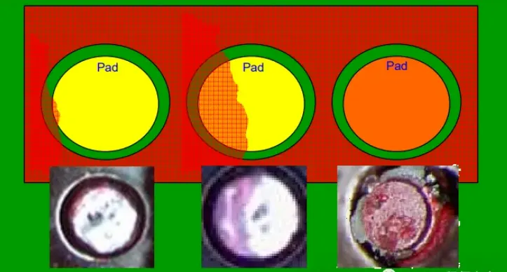
SMT BGA Failure Analysis by Dye Stain: Procedure, Criteria, and Practical Cases
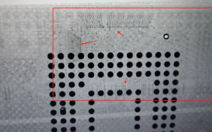
X-Ray Inspection of eMMC BGA: Solder Ball Assessment and an Unexpected Finding
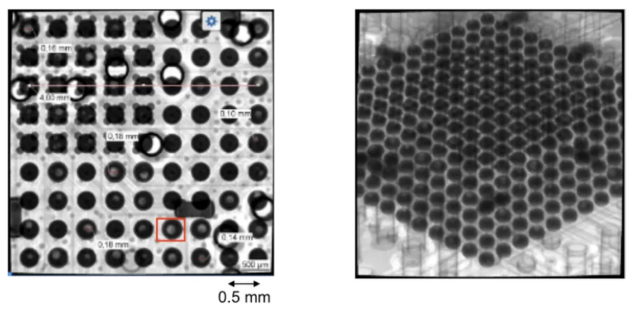
Troubleshooting PCB Assembly with X Ray: A Practical Guide for Engineers
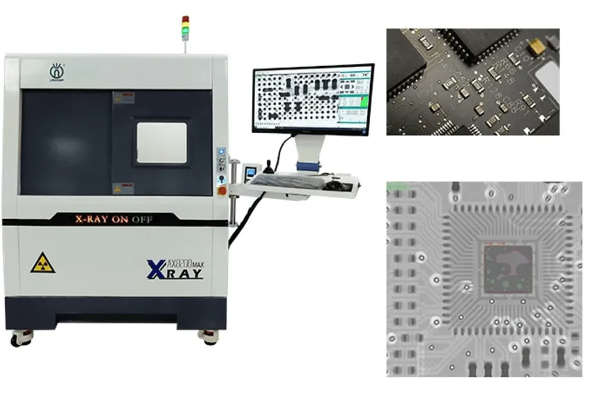
From Voids to Misalignments: A Complete Guide to PCB X Ray Inspection
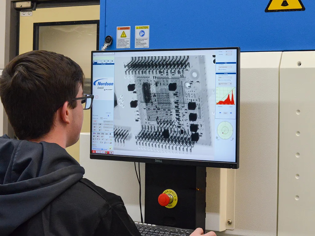
X Ray Vision for PCBs: Mastering Defect Detection in Electronics Manufacturing

HDI PCB X-Ray Inspection for Assemblies: SMT Defect Detection and Quality Control
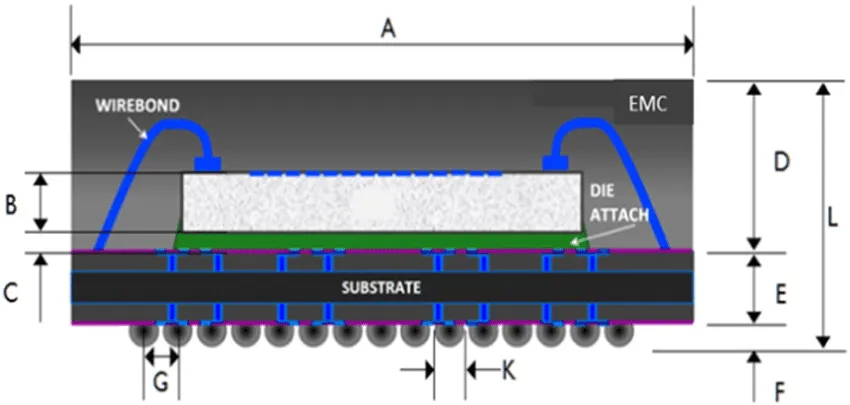
BGA Inspection Demystified: How X Ray Technology Ensures Reliable Solder Joints
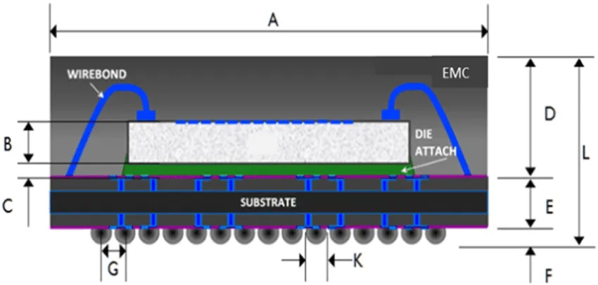
A Comprehensive Guide to BGA Assembly and Inspection

Uncovering Hidden PCB Defects: A Guide to BGA X-Ray Inspection