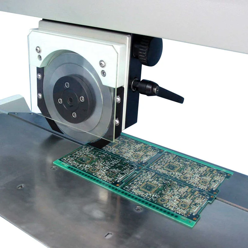
Depaneling Cost
Depaneling is a critical step in printed circuit board (PCB) manufacturing, where individual boards are separated from a larger production panel. For professionals in electronics design and production, understanding depaneling cost is essential to optimizing budgets and ensuring efficient workflows. This tag page aggregates articles that delve into the various factors influencing depaneling expenses, from method selection to material considerations, helping you make informed decisions that balance quality and affordability. Key elements affecting depaneling cost include the choice of techniques such as routing, laser cutting, or v-scoring, each with its own implications for time, labor, and equipment investment. For instance, manual methods might suit low-volume prototypes but can escalate costs in high-volume runs due to increased labor and potential for errors. Automated approaches, while initially more expensive, often reduce long-term expenditures by minimizing waste and improving precision. Articles under this tag explore these trade-offs, offering practical insights like calculating total cost of ownership and strategies for selecting vendors that align with your project scale. By examining real-world case studies and best practices, you can apply actionable tips to lower depaneling costs without compromising board integrity. This might involve designing panels with optimal tab placements or integrating depaneling into early prototyping phases to avoid costly revisions. Whether you are a PCB engineer seeking to streamline production or a manufacturer evaluating process efficiencies, the resources here provide valuable guidance. Browsing through the linked articles can further illuminate specific scenarios, such as cost comparisons for flexible versus rigid PCBs, empowering you to enhance your manufacturing strategies.
Video Guide
No videos found for this tag.
Technical Articles
Get in Touch
Send Message
- Products & Service
- Company
- About AIVON
- Contact
- News
- Blog
- Certification
-


- Payment
-


2026 AIVON.COM All Rights Reserved