Dog-Bone Routing
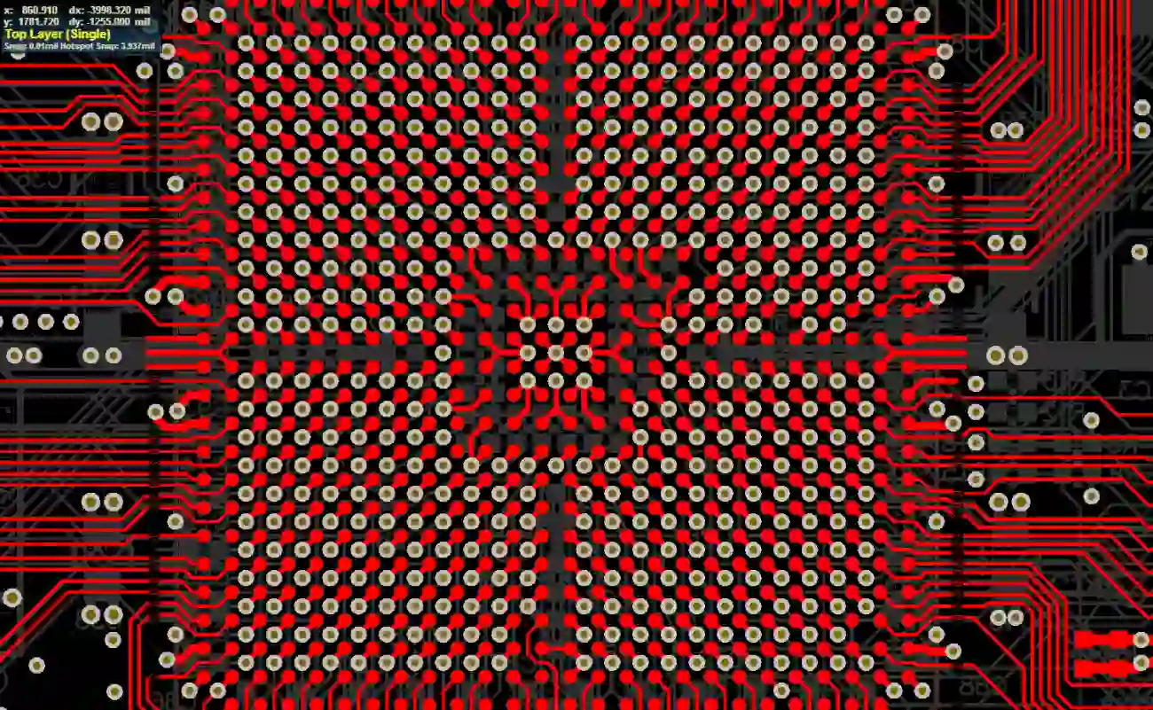
Dog-bone routing is a specialized technique in printed circuit board (PCB) design, particularly valuable for managing high-density interconnects in ball grid array (BGA) packages. This method involves placing vias slightly offset from the BGA pads and connecting them with short, straight traces, creating a shape reminiscent of a dog bone. By doing so, it facilitates efficient signal escape from the inner rows of densely packed BGA balls, where direct via-in-pad placement might not be feasible due to manufacturing constraints or signal integrity concerns. For engineers and designers searching for dog-bone routing solutions, this approach offers several practical benefits. It minimizes layer count in multi-layer PCBs by optimizing via placement, reduces crosstalk and electromagnetic interference, and enhances overall board reliability. In applications like consumer electronics, telecommunications, and automotive systems, where space is at a premium and performance is critical, dog-bone routing enables tighter layouts without compromising electrical performance. Best practices include maintaining consistent trace widths to match impedance requirements, ensuring adequate clearance between vias to prevent shorts, and using simulation tools to verify signal paths before fabrication. Common pitfalls to avoid involve overlooking thermal relief in power planes or neglecting drill size tolerances, which can lead to assembly issues. This tag gathers in-depth articles that delve into real-world implementations of dog-bone routing, from beginner tutorials on CAD software integration to advanced case studies on high-speed designs. Readers can find guidance on selecting appropriate via types, integrating this technique with fanout strategies, and troubleshooting common errors in prototype iterations. By applying these insights, designers can streamline their workflows and achieve more robust PCB outcomes in demanding projects.
Video Guide
No videos found for this tag.
Technical Articles
Get in Touch
Send Message
- Products & Service
- Company
- About AIVON
- Contact
- News
- Blog
- Certification
-


- Payment
-


2026 AIVON.COM All Rights Reserved