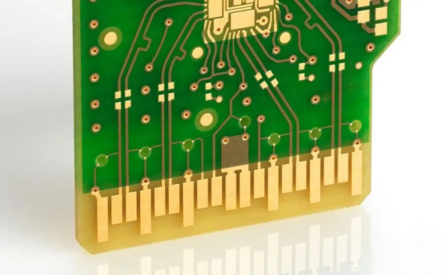
PCB Handling
Proper handling of printed circuit boards (PCBs) is essential for maintaining their integrity and ensuring reliable performance in electronic devices. The PCB Handling tag encompasses a range of topics focused on the safe and effective management of PCBs throughout their lifecycle, from manufacturing and assembly to storage and transportation. For engineers, technicians, and hobbyists searching for guidance on PCB Handling, this collection of articles provides practical strategies to minimize risks such as electrostatic discharge (ESD), physical damage, and contamination, which can lead to costly failures or reduced lifespan. Understanding the fundamentals of PCB Handling begins with implementing ESD-safe practices. Always use grounded wrist straps, antistatic mats, and ionized air blowers to dissipate static charges that could harm sensitive components. When manually handling PCBs, grip them by the edges to avoid touching traces or solder pads, and wear clean gloves to prevent oils and residues from transferring. For storage, opt for antistatic bags or containers in controlled environments with stable temperature and humidity levels to prevent warping or corrosion. In assembly lines, automated handling systems can reduce human error, but even then, regular training on best practices ensures consistency and quality. These insights are particularly valuable for those troubleshooting common issues like intermittent faults caused by improper handling or seeking ways to optimize workflows in prototyping and production. By applying these techniques, you can enhance product reliability and efficiency. The articles linked under this tag delve deeper into specific scenarios, such as handling multilayer boards or preparing PCBs for soldering, offering detailed advice tailored to real-world applications. Whether you are scaling up manufacturing or refining a personal project, reviewing these resources can help you adopt proven methods that safeguard your electronics investments.
Video Guide
No videos found for this tag.
Technical Articles
Get in Touch
Send Message
- Products & Service
- Company
- About AIVON
- Contact
- News
- Blog
- Certification
-


- Payment
-


2026 AIVON.COM All Rights Reserved