RF PCB Stack-Up
RF PCB stack-up refers to the strategic layering of materials and conductive traces in printed circuit boards designed for radio frequency applications. This configuration is essential for maintaining signal integrity, controlling impedance, and minimizing electromagnetic interference in high-frequency circuits. Engineers and designers searching for information on RF PCB stack-up often seek guidance on optimizing board performance for devices like wireless communication systems, radar modules, and IoT sensors, where even minor deviations can lead to signal degradation or failure. Understanding the fundamentals of RF PCB stack-up begins with selecting appropriate dielectric materials, such as low-loss laminates like Rogers or FR-4 variants, to achieve desired electrical properties. Best practices include balancing layer counts to support differential signaling, incorporating ground planes for shielding, and calculating trace widths for controlled impedance. For instance, a typical four-layer stack-up might feature signal layers separated by prepreg and core materials to reduce crosstalk, while advanced designs could integrate microvias for denser routing in compact RF modules. These approaches not only enhance reliability but also streamline manufacturing processes, reducing costs and time to market. Professionals in electronics design can benefit from exploring articles tagged under RF PCB stack-up, which delve into real-world examples, simulation techniques using tools like HFSS or Altium, and troubleshooting common issues such as parasitic capacitance. Whether you are refining a prototype or scaling production, these resources provide practical insights to implement effective stack-up strategies tailored to specific frequency bands and environmental conditions. By applying these principles, designers can ensure robust performance in demanding RF environments.
Technical Articles
Antenna Design and Integration for RF PCBs: Fundamentals, Types, Radiation Patterns, and Manufacturing Considerations
Types of Radar Jamming Techniques
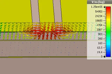
5G Telecommunication Base Station PCB Design: Challenges and Solutions for Millimeter Wave Frequencies
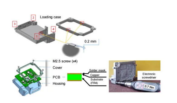
Advanced Techniques for Hybrid Stack Up Design in RF Laminate PCBs
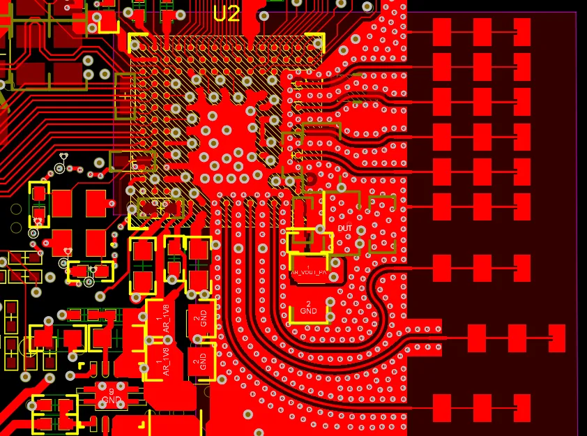
RF PCB Design for Beginners: A Complete Introductory Guide

Spectrum Analyzers and Network Analyzers for RF PCB Design, Signal Integrity, and High-Frequency Manufacturing Validation
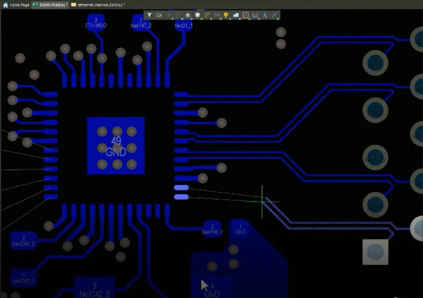
Optimizing PCB Stack Up for RF Applications: A Practical Guide

Cellular Mobile Technology: PCB Design and Manufacturing for 4G/5G Networks
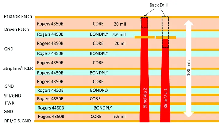
High Layer Count PCB Stackup Design for RF Applications: Minimizing Signal Loss