Silkscreen Legibility
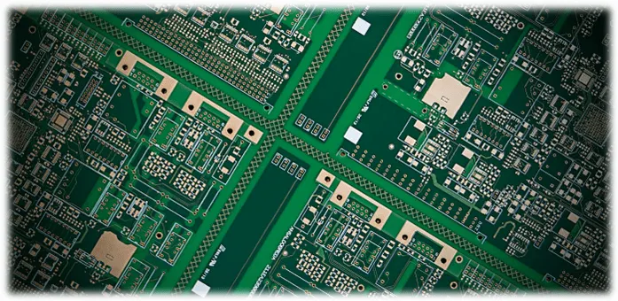
Silkscreen legibility plays a crucial role in printed circuit board design, ensuring that text, symbols, and markings on the PCB surface remain clear and readable throughout the manufacturing, assembly, and maintenance processes. This aspect focuses on the quality of the silkscreen layer, which includes component labels, polarity indicators, and reference designators. Poor legibility can lead to assembly errors, increased debugging time, or even compliance issues in regulated industries like aerospace and medical devices. For engineers and hobbyists searching for ways to enhance PCB readability, understanding silkscreen legibility helps in selecting appropriate fonts, sizes, and contrasts that withstand soldering, cleaning, and environmental stresses. Key best practices for achieving optimal silkscreen legibility include using sans-serif fonts with a minimum height of 0.8mm to prevent blurring during printing, maintaining high contrast between the silkscreen ink and the board's solder mask, and avoiding overcrowding by prioritizing essential markings. Designers should also consider fabrication limitations, such as the resolution of the silkscreen process, to ensure markings remain intact on fine-pitch boards. By applying these techniques, you can reduce production rejects and improve the overall reliability of your electronic projects. For instance, testing legibility under various lighting conditions or using software tools to simulate silkscreen output can provide actionable insights before committing to fabrication. Articles tagged under Silkscreen Legibility offer in-depth guidance on these topics, from beginner tips for hobbyist PCB layouts to advanced strategies for high-density designs. Browsing through them can help you refine your approach and address specific challenges in your work.
Video Guide
No videos found for this tag.
Technical Articles
Get in Touch
Send Message
- Products & Service
- Company
- About AIVON
- Contact
- News
- Blog
- Certification
-


- Payment
-


2026 AIVON.COM All Rights Reserved