 00:54
00:54
Through-Hole Plating
Through-hole plating is a fundamental process in printed circuit board (PCB) manufacturing that involves depositing a conductive layer inside drilled holes to establish reliable electrical connections between different layers of the board. This technique ensures that components mounted via through-hole technology can securely interface with the PCB's internal circuitry, enhancing overall durability and signal integrity. For engineers, hobbyists, and manufacturers searching for insights on through-hole plating, this tag serves as a comprehensive resource, covering everything from basic principles to advanced implementation strategies. Understanding through-hole plating begins with its role in multilayer PCBs, where it prevents issues like signal loss or mechanical failure by creating robust vias. Common methods include electroless copper deposition followed by electroplating, which provide a uniform conductive coating. Practical applications span consumer electronics, automotive systems, and industrial equipment, where reliability under thermal stress or vibration is critical. Best practices emphasize precise drilling tolerances, proper bath chemistry control, and post-plating inspections to avoid defects such as voids or uneven plating thickness. By adhering to these guidelines, designers can optimize board performance and reduce rework costs. For those troubleshooting plating-related challenges or seeking to integrate this process into their projects, our curated articles offer detailed case studies and step-by-step tutorials. Whether you are comparing through-hole plating to surface-mount alternatives or exploring innovations like additive manufacturing integrations, these resources provide actionable advice to refine your PCB designs. Readers often find value in related topics such as via filling techniques or material selection, which build on the foundational knowledge presented here.
Video Guide
-
00:54
Technical Articles
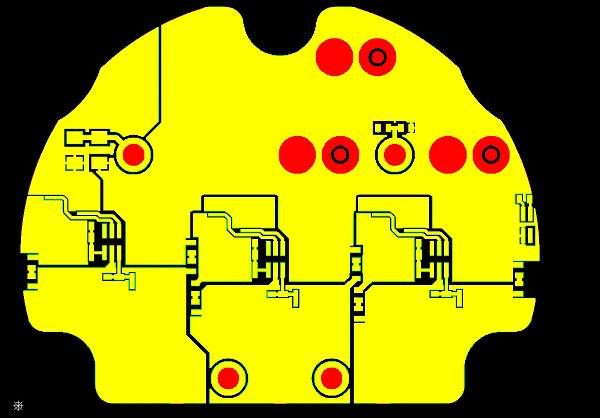
Why PCB CAM Must Verify PTH and NPTH Hole Definitions
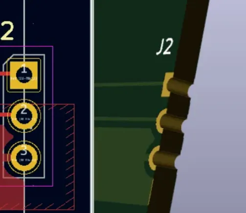
Designing PCB Castellated Holes with KiCad
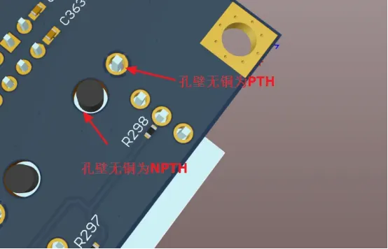
PTH and NPTH on a PCB: How to Tell the Holes Apart

Press-Fit Interconnects for Electronics: Principles, Materials, Process, and Controls
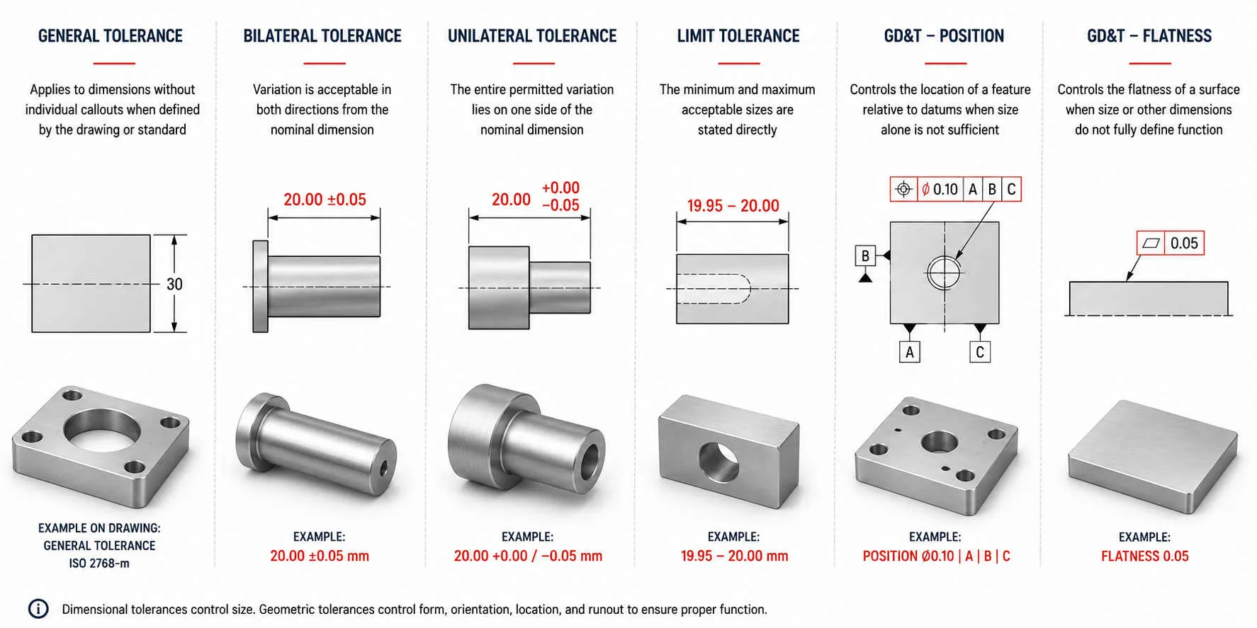
Hole Design Guidelines for CNC Machining
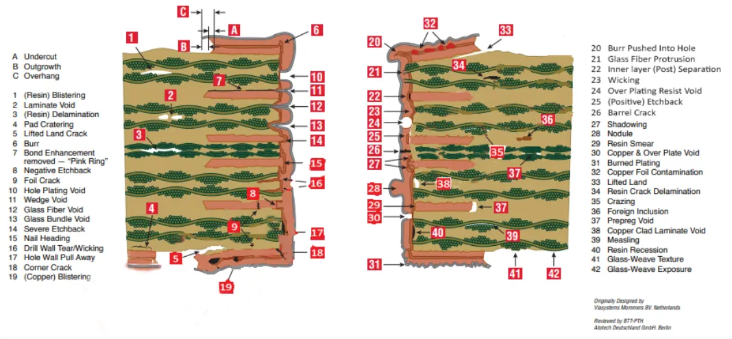
Choosing the Right Plating Material for Your Plated Through-Holes
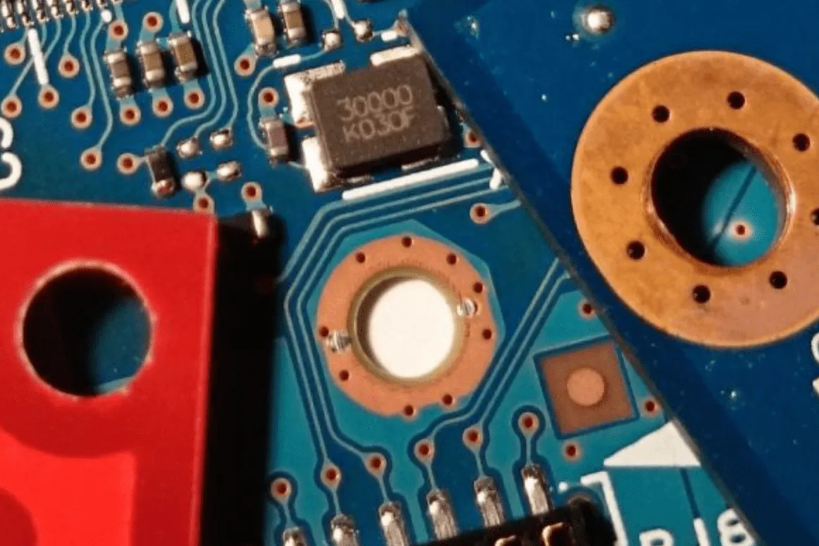
PTH vs NPTH: Defining the Core Difference
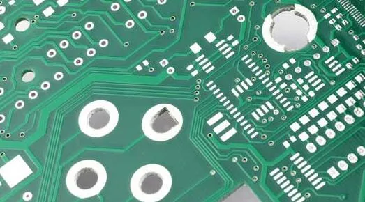
How to Repair Damaged Plated Through-Holes (PTH) on a PCB
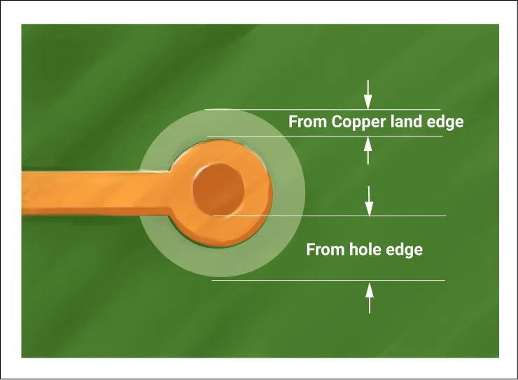
Enhancing Plated Through-Hole Current Capacity in High-Power PCBs
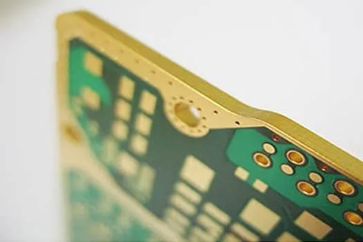
Solving Plated Through-Hole Problems: A PCB Troubleshooting Guide

FR4 PCB Plated Through-Hole Reliability: Common Risks and Controls