Via Alternatives
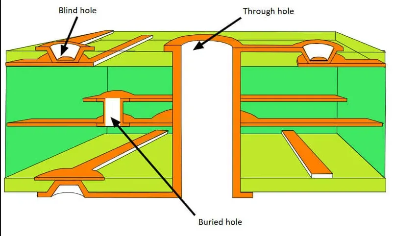
In the realm of printed circuit board (PCB) design, vias serve as essential conduits for connecting multiple layers, but they can introduce challenges such as signal integrity issues, manufacturing complexity, and increased costs. The Via Alternatives tag explores innovative strategies and techniques to minimize or eliminate the need for traditional vias, enabling engineers and designers to optimize their layouts for performance and efficiency. Whether you are dealing with high-speed digital circuits, dense multilayer boards, or space-constrained applications, understanding these alternatives can significantly enhance your design process. One common approach involves blind and buried vias, which reduce layer transitions without penetrating the entire board, thereby preserving signal paths and reducing electromagnetic interference. Another effective method is the use of microvias in high-density interconnect (HDI) designs, offering finer pitch and better thermal management compared to standard through-hole vias. For even more advanced solutions, designers often turn to via-in-pad techniques or alternative routing strategies like fanout patterns and layer stacking optimizations. These methods not only streamline fabrication but also improve reliability in demanding environments, such as automotive electronics or telecommunications equipment. By adopting Via Alternatives, you can achieve actionable benefits like lower production costs, faster time-to-market, and superior board performance. Best practices include conducting thorough simulations to evaluate signal integrity before implementation and selecting materials that support alternative via structures. For those seeking deeper insights, the articles linked under this tag provide detailed case studies and step-by-step guides on integrating these techniques into real-world projects, helping you refine your PCB designs with confidence.
Video Guide
No videos found for this tag.
Technical Articles
Get in Touch
Send Message
- Products & Service
- Company
- About AIVON
- Contact
- News
- Blog
- Certification
-


- Payment
-


2026 AIVON.COM All Rights Reserved