Overview
The original project was developed at CERN. For a particular experiment they needed a large number of precision voltmeters, and because commercial instruments were expensive they decided to build their own.
CERN Multimeter Project
The design includes an eight-and-a-half digit meter intended for laboratory use. The circuit is not conceptually complex but emphasizes reliability features such as temperature protection.
Uses an ADC.
This is the core board.
Interior view; the large IC is an FPGA.
Final assembled unit.
F-ammeter.
Circuit Descriptions
1. Power circuit: The design uses two LM1117 LDO regulators in series. The first stage converts the input to a 5V output; the second stage converts 5V to 3.3V to supply the system modules.
2. Voltage detection circuit: One LM324 op amp is used in three roles to implement amplifier, attenuator, and buffer stages for different input voltage ranges. The op amp outputs are connected to a CD4052 analog switch for range selection.
3. Current detection circuit: A current-sensing amplifier such as MAX4080 is used with a gain of 20. Relay switching selects different sense resistors for range changes.
4. Resistance measurement circuit: Resistor measurement is implemented with voltage division and MOSFETs to select different scaling resistors.
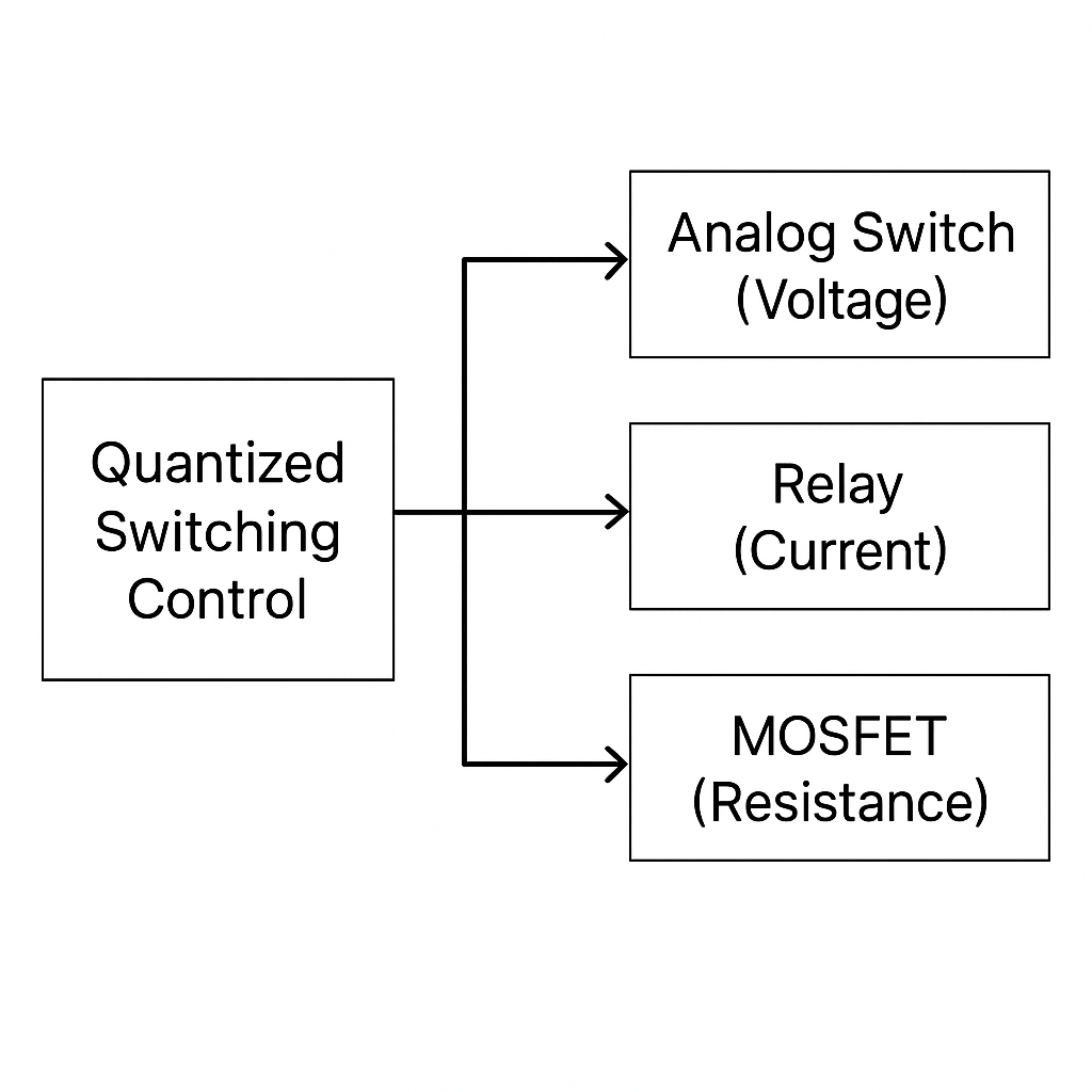
Range switching functionality is implemented as shown below.
Electronic switches used for range selection.
Classic transistor circuits and protection circuitry are used.
Resistance measurement stage.
Op amp buffering stage.
Another open hardware design with available documentation.
Screenless Multimeter Reference
The following design is a screenless multimeter.
Schematic.
Typical connections.
PCB layout.
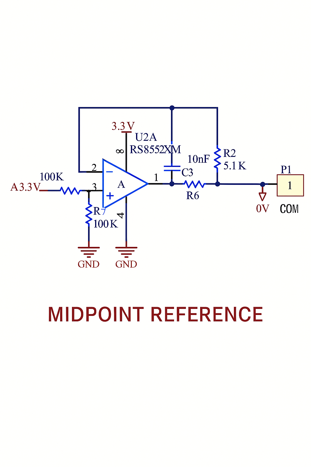
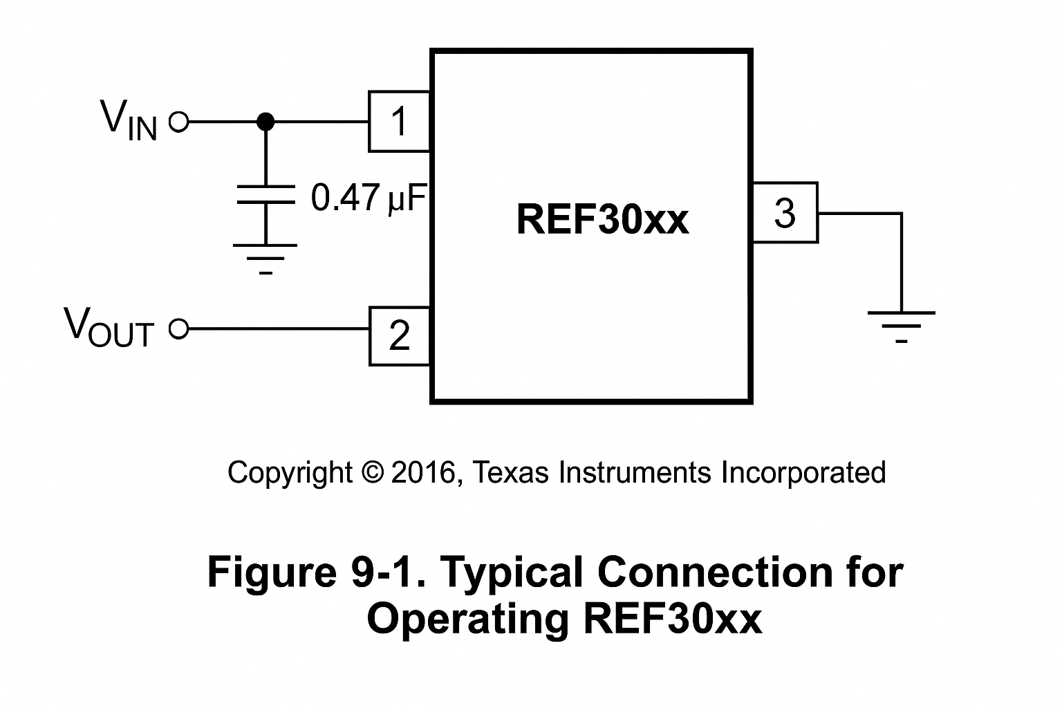
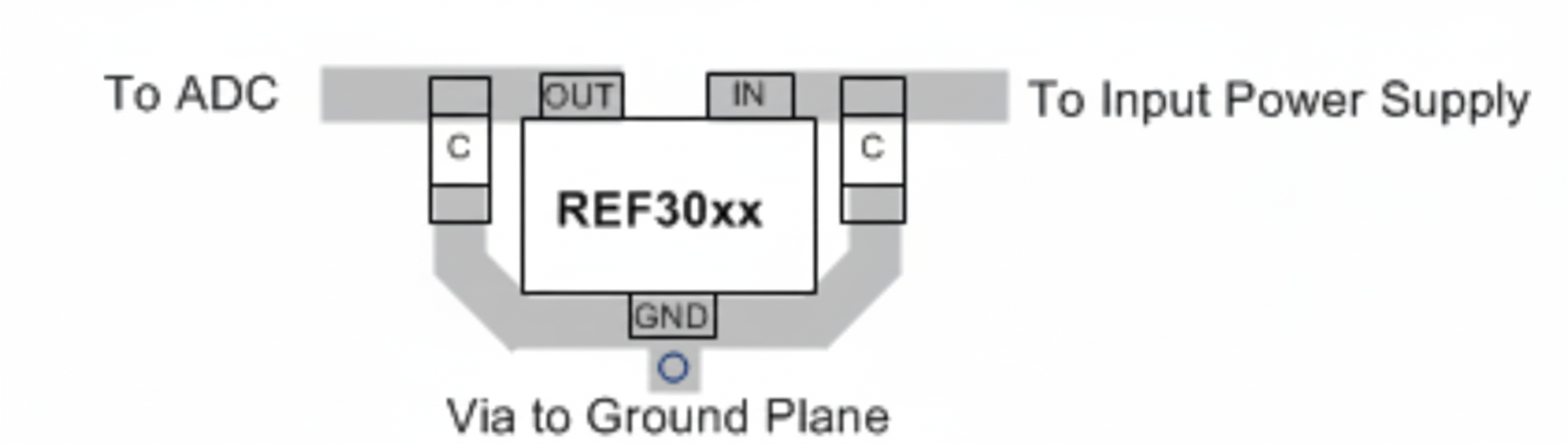
Reference Voltage and Signal Chain
The reference voltage (VREF) is important and often essential in high-precision signal chain applications. Standard signal chains typically include a data converter such as an ADC or a DAC. Many signal-chain applications are sensitive to gain or noise errors, so the reference output used by the converter is usually the most accurate voltage available to the data converter.
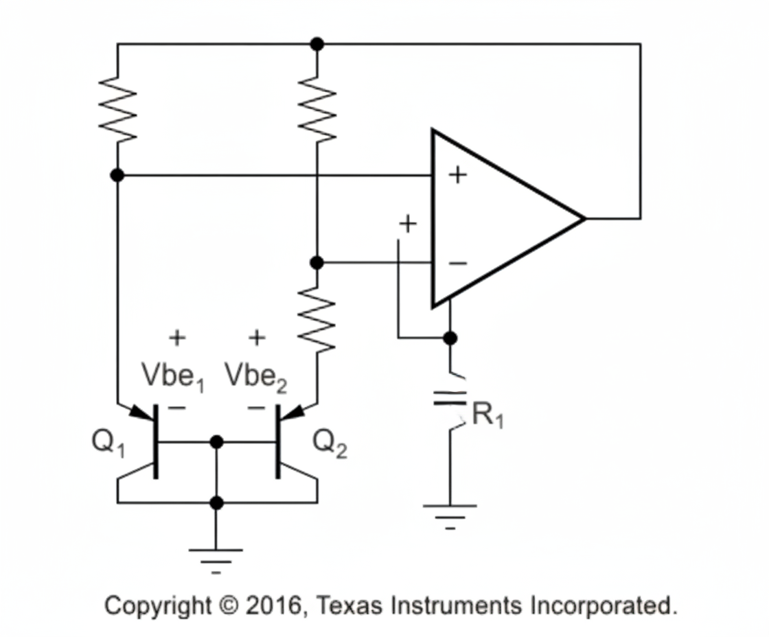
Current mirror illustration.
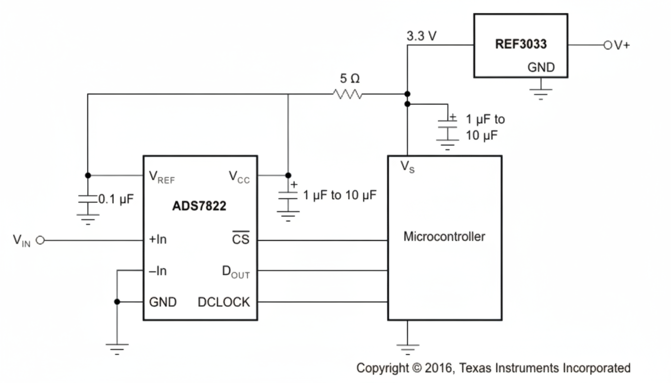
Example reference chip usage.
Reference placement and REF pin locations.
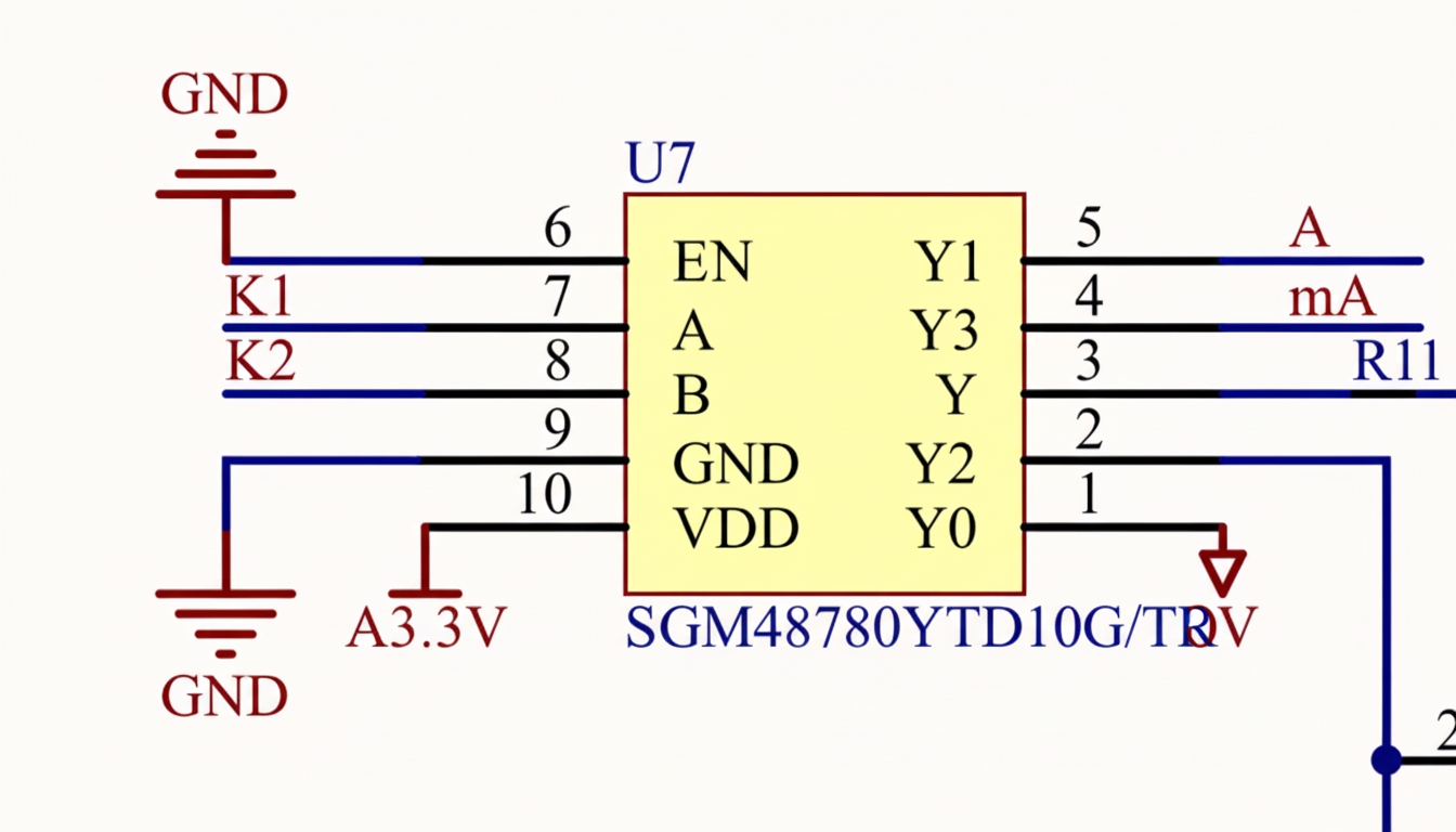
A 4-bit electronic switch is used for dynamic range switching; the source code implements this function. Relays can serve the same purpose.
IO connections are shown here.
Dual-channel switch.
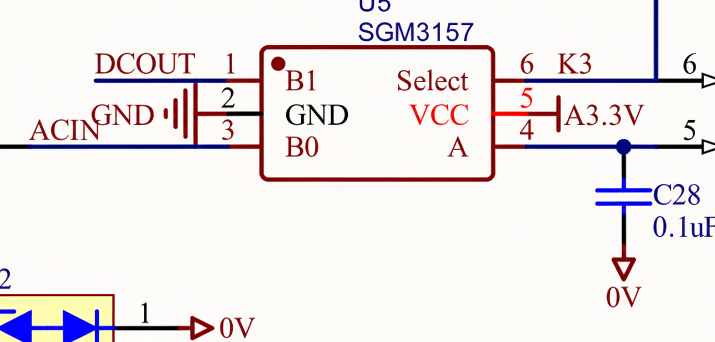
Analog Switches
SGM3157 is a CMOS analog switch with low power consumption, low propagation delay, and low on-resistance. The analog and digital signal output ranges span from VCC to GND. The select input has overvoltage protection, allowing the select input to exceed VCC up to 7V without damaging the pin.
Functional diagram.

ESP32-S2 DAC and Relay Control
S2 contains two 8-bit DAC channels that convert two digital signals into two analog voltage outputs; the channels operate independently. Each DAC consists of an internal resistor ladder and a buffer. The DAC reference voltage is VDD3P3_RTC_IO. The DAC outputs are used to control relays for range switching.
Further analysis of this section will be provided in a follow-up.
These locations use electronic switches to perform dynamic switching.
Current measurement stages convert current to voltage for ADC measurement.
MCP3421 ADC
The MCP3421 uses the I2C serial interface. It is a single-channel, high-precision ADC supporting up to 18-bit resolution with differential input. The on-chip precision reference is 2.048V. It operates from a single supply (2.7V to 5.5V).
The design uses an external ADC rather than relying on the microcontroller's internal ADC.
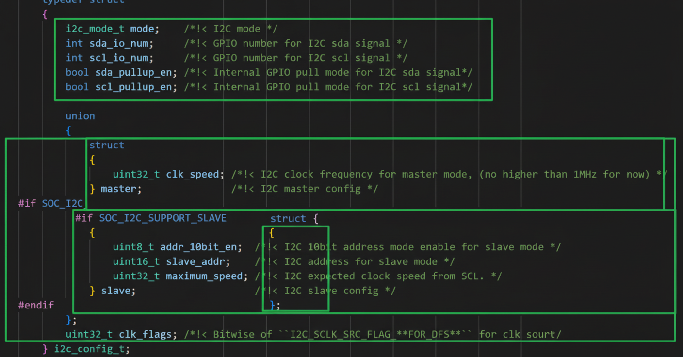
I2C on ESP32-S2
ESP32-S2 provides two hardware I2C controllers. The design shows the detailed I2C structure and typical read/write sequences. Firmware implements write-then-read operations for the external ADC.

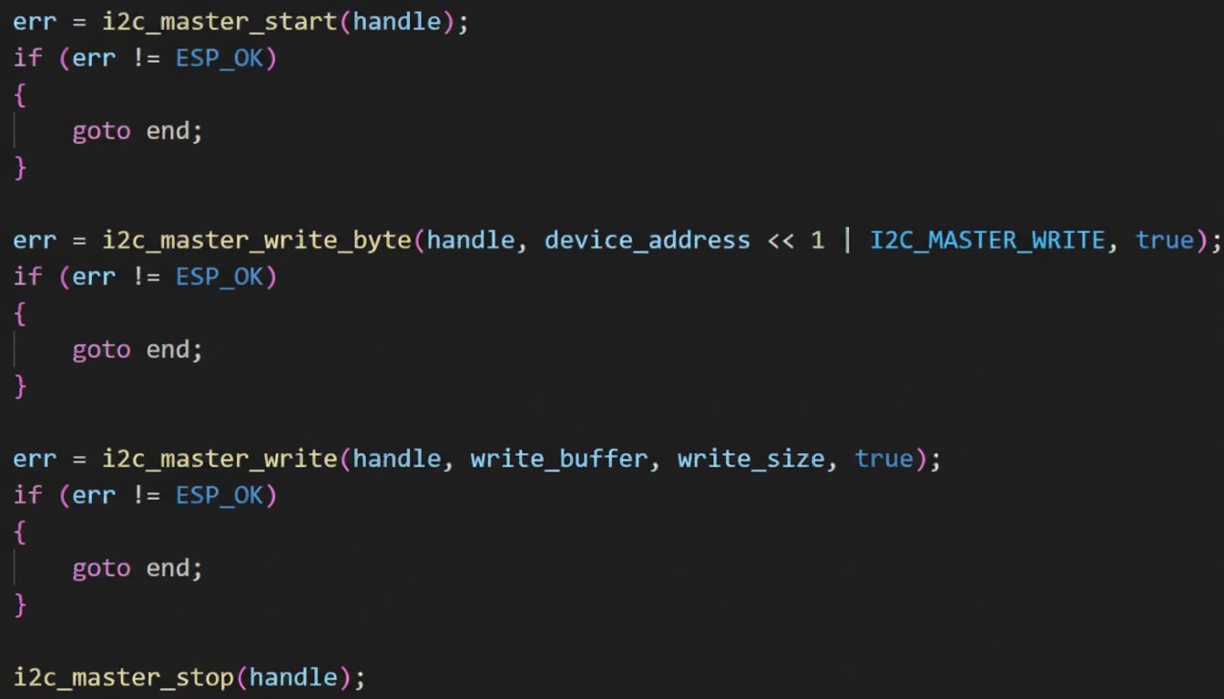
Typical write-then-read I2C transaction diagram.
Firmware and Source Code
The source repository includes code for IoT-related functions, but some modules were not located in the reviewed copy.
The provided firmware improves functionality for measurement and control.
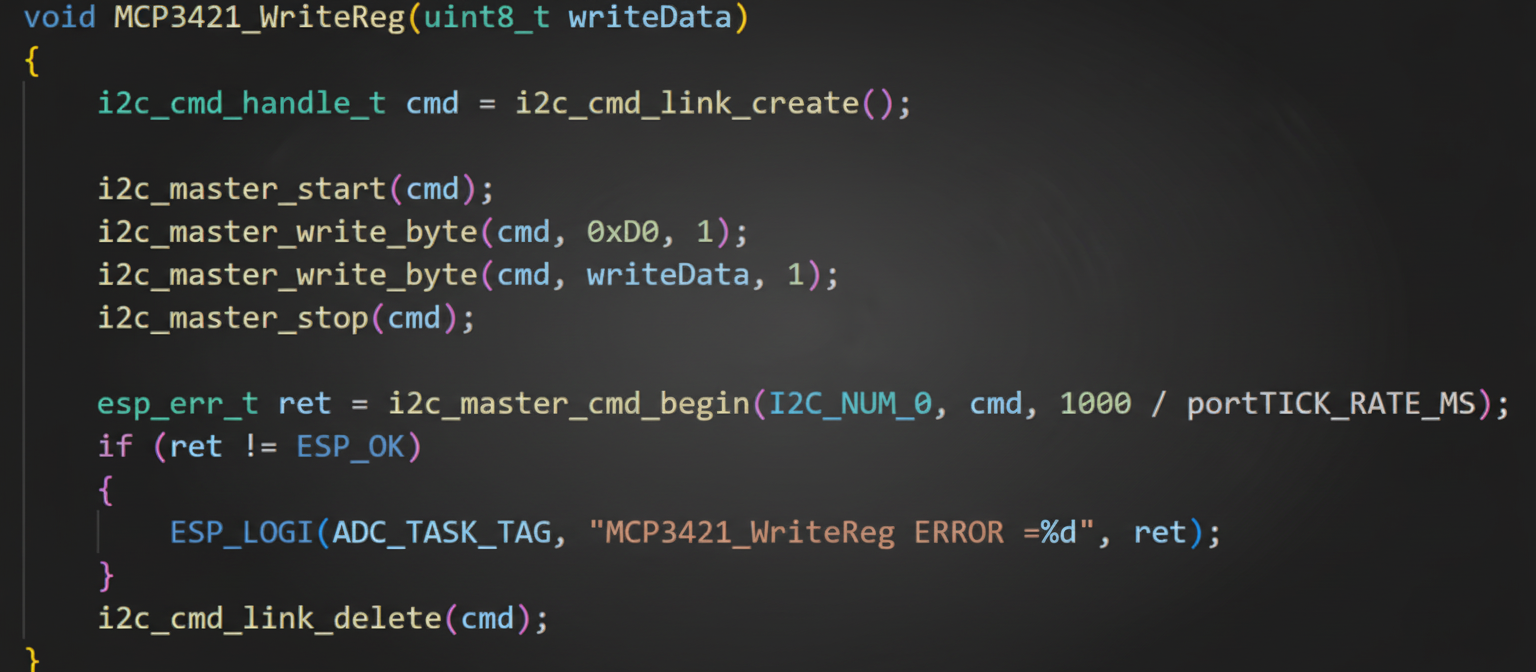
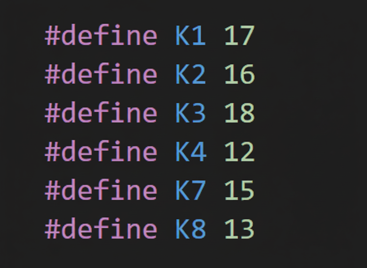
Example: MCP3421 write function wrapper and range conversion functions are implemented in the codebase. Electronic switch pin mappings and trigger behavior (active-high) are documented.
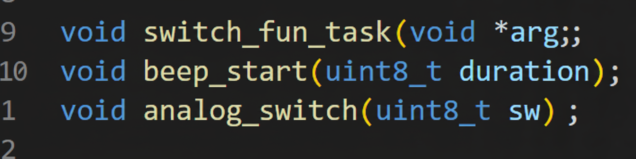
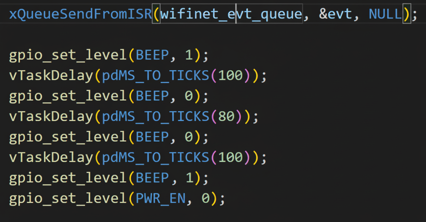
Control button handling and synchronous beep trigger are shown in the control flow diagrams.