Back-illuminated (BSI) CMOS image sensors reverse the conventional layer order of front-side illuminated (FSI) designs to increase light collection efficiency. Stacked CMOS architectures further separate pixel and circuit fabrication before bonding. Both approaches address fundamental area and optical constraints in modern imaging devices while introducing specific requirements for sensor packaging and supporting electronics.
Front-Illuminated CMOS Structure and Limitations
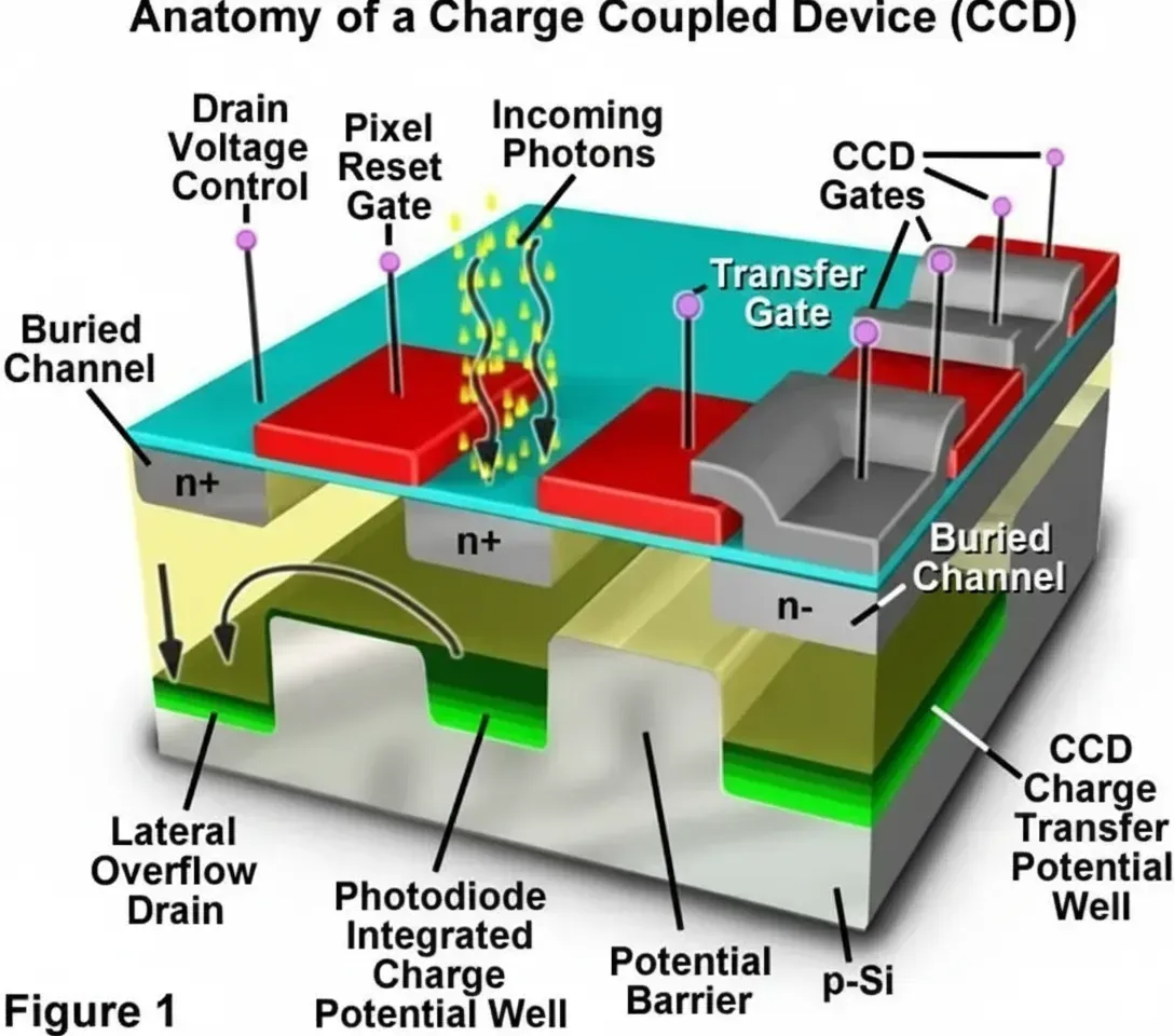
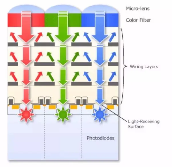
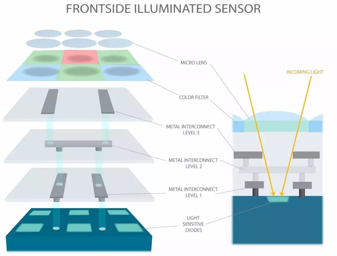
In a conventional FSI sensor the layer stack from the light-incident side consists of microlenses, color filter array, metal interconnect wiring, and photodiodes. Photodiodes and readout circuitry compete for pixel real estate; larger circuit blocks reduce photodiode area and therefore light collection. Incident light must also traverse the opaque metal layers, resulting in partial blockage, reflection, and potential crosstalk between pixels. These factors limit sensitivity, raise noise at high ISO settings, and constrain readout speed when column-parallel ADCs and amplifiers occupy significant area.
Back-Illuminated CMOS Structure and Advantages
BSI sensors relocate the wiring layer beneath the photodiode layer. Light reaches the photodiodes directly after passing only through the microlenses and color filters, increasing the effective fill factor. The larger photodiode area improves quantum efficiency and signal-to-noise ratio, particularly under low-light conditions. Circuitry no longer competes with the photosensitive area, permitting denser or more sophisticated readout electronics that support higher frame rates, burst capture, and advanced video modes.
BSI sensors also accept oblique rays more effectively, reducing the need for aggressive microlens optimization at the sensor edges. Trade-offs include potentially higher electrical crosstalk between densely packed circuits and minor sensitivity penalties at very low ISO values. Overall, BSI designs deliver measurable gains in low-light performance and autofocus speed compared with equivalent FSI sensors.
Stacked CMOS Architecture
Stacked sensors separate the pixel array and the readout/processing circuitry onto distinct wafers fabricated on optimized process nodes. After independent processing—including thermal annealing for the pixel layer—the wafers are bonded using techniques that exploit differences in thermal expansion or intermediate layers. The resulting stack retains the back-illuminated pixel orientation while allowing the circuit layer to use finer process nodes for higher transistor density and lower power.
This separation avoids thermal damage to pre-formed circuits during pixel annealing and removes process-node compromises. Additional features such as per-row exposure control for hardware HDR and RGBW pixel arrangements become practical. Stacked designs also enable thinner modules by reducing the lateral footprint required for circuitry.
Performance Characteristics and Selection Considerations
BSI and stacked sensors improve light sensitivity by approximately 30–50 % in low-light conditions relative to earlier FSI generations, although final image quality also depends on lens optics and downstream image-signal processing. Large-format sensors (APS-C or full-frame) present lower manufacturing yields when adopting BSI or stacked processes, limiting adoption until defect densities improve. At low ISO values, performance differences between BSI/stacked and conventional sensors are often small; advantages become pronounced at high ISO and in low-light autofocus.
Design and Manufacturing Considerations
BSI fabrication requires precise wafer thinning, backside passivation, and alignment accuracy during bonding or stacking. Stress management is critical to prevent warping or delamination that could affect pixel uniformity. Thermal budgets during bonding must preserve circuit performance while repairing pixel-layer damage. Yield scaling with sensor size directly influences cost, especially for large die. Environmental qualification includes thermal cycling, mechanical shock, humidity, and light-stress testing to verify long-term stability of microlenses, color filters, and bonded interfaces.
Industry Trends and System Integration
Smartphone and compact camera platforms continue to adopt BSI and stacked sensors to achieve higher resolution, faster readout, and improved low-light capability within shrinking module volumes. Integration with on-sensor HDR, multi-frame noise reduction, and high-speed interfaces (MIPI CSI-2, C-PHY) increases the complexity of the supporting electronics. These trends emphasize design-for-manufacturability practices that balance optical performance, electrical signal integrity, and mechanical robustness across temperature and vibration ranges.
PCB and Electronic Manufacturing Relevance
High-performance image sensor modules rely on advanced PCB and flexible circuit technologies. MIPI or other high-speed serial interfaces demand controlled-impedance routing, low-loss dielectrics, and precise via structures to maintain signal integrity at multi-gigabit rates. Power delivery networks must supply clean, low-noise voltage to analog front-ends and ADCs while managing heat from processors and illumination sources. Flexible printed circuits (FPC) enable compact, vibration-resistant camera modules that fold around lens barrels or conform to curved housings. High-density interconnect (HDI) substrates support dense ball-grid-array or chip-on-board sensor packaging. Metal-core or copper core PCBs provide thermal solutions for high-power stacked sensors. Material selection—substrate Tg, coefficient of thermal expansion matching, surface finishes, and conformal coatings—directly affects long-term reliability under automotive or industrial environmental stresses. Manufacturing processes such as laser drilling, fine-line etching, and automated optical inspection parallel the precision requirements of sensor wafer processing.
These PCB capabilities allow electronics suppliers to deliver reliable camera modules, sensor interface boards, and integrated imaging assemblies that meet the stringent performance and qualification standards of mobile, automotive, and machine-vision applications.
Conclusion
Back-illuminated and stacked CMOS sensors overcome the optical and area limitations of traditional front-illuminated designs through layer reordering and wafer-level bonding. Realizing their performance benefits in practical systems depends on precise control of thinning, bonding, and thermal processes, as well as robust electronic interfaces. PCB fabrication, assembly, and material engineering practices underpin the high-speed data paths, power integrity, thermal management, and mechanical flexibility required for dependable imaging modules across consumer, industrial, and automotive platforms.