Advanced memory technologies such as spin-orbit torque MRAM (SOT-MRAM), one-time programmable (OTP) eFuses, 3D stacked DRAM, and sub-nanometer CMOS logic are reshaping system architectures for AI, automotive, and high-performance computing. While these innovations primarily target the silicon level, their successful deployment in production systems depends on printed circuit board (PCB) design that addresses high-speed signaling, power integrity, thermal dissipation, and long-term reliability. Effective PCB engineering bridges the gap between emerging memory devices and robust, manufacturable end products.
SOT-MRAM and Low-Power Non-Volatile Memory on the PCB
TSMC's SOT-MRAM achieves approximately one-tenth the write power of conventional spin-transfer torque MRAM while maintaining high endurance and speed. This makes it attractive for cache, embedded storage, and edge AI applications where frequent writes must occur without excessive energy consumption.
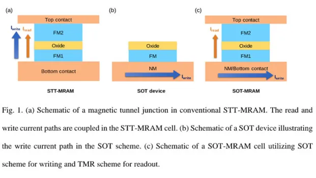
On the PCB, SOT-MRAM's lower power profile reduces the demands on voltage regulator modules and power delivery networks. Designers can employ thinner copper planes and simpler decoupling strategies while still meeting strict noise margins. However, the technology's sensitivity to magnetic fields requires careful PCB layout to avoid external interference—typically achieved through ground planes, shielding layers, and strategic component placement. Signal integrity for the high-speed interfaces connected to SOT-MRAM remains critical, often necessitating low-loss laminates and controlled-impedance routing to preserve data integrity at multi-Gbps rates.
OTP Memory and eFuse Implementation in PCB Designs
One-time programmable memory using eFuses provides secure, permanent storage for configuration data, calibration values, and security keys. Programming typically requires elevated voltages (often 5–10 V) and precise current control, which directly influences PCB power architecture.
Designers must allocate dedicated high-voltage traces or planes with appropriate clearance and creepage distances. Robust decoupling and current-limiting components protect both the fuse and surrounding circuitry. Because eFuses are irreversible, PCB layouts often incorporate redundant programming paths or external programming headers to support manufacturing and field updates. Thermal management during programming prevents localized heating that could affect nearby sensitive components or cause delamination in the board.
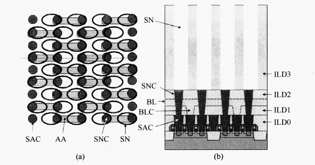
3D Stacked DRAM and High-Bandwidth Memory Interfaces
Stacked DRAM architectures increase density and bandwidth by vertically integrating multiple memory dies, reducing the physical footprint and shortening interconnect lengths. These structures are commonly paired with high-bandwidth memory (HBM) or similar interfaces in advanced packaging.
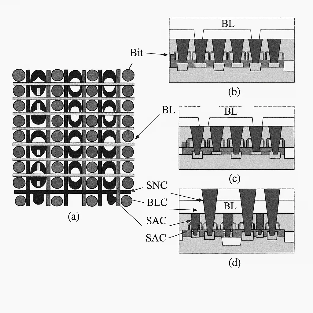
From a PCB perspective, 3D stacked DRAM demands exceptional signal integrity and power delivery. HBM-style interfaces operate at multi-Gbps per pin, requiring precise stack-up design with low-Dk/Df materials, minimal via stubs, and optimized return paths. Via-in-pad and back-drilling techniques become essential to maintain clean eye diagrams. Thermal management grows more challenging as heat from dense stacks must be extracted through the HDI PCB; thick copper planes, thermal vias, and sometimes metal-core or embedded heat-spreader solutions are employed. Power integrity simulations must account for simultaneous switching noise across hundreds of I/O pins.
CMOS Logic Scaling to 3D Sub-Nanometer Nodes and PCB Implications
Continued CMOS scaling into sub-3 nm and 3D-stacked transistor architectures increases transistor density and performance but also raises challenges in packaging and board-level integration. Finer process nodes produce faster edge rates and higher current densities, translating into stricter requirements for PCB trace impedance, crosstalk control, and electromagnetic compatibility.
Designers increasingly adopt HDI (high-density interconnect) features, sequential lamination, and advanced surface finishes to support fine-pitch packages. Low-loss dielectrics help preserve signal quality at higher frequencies, while improved thermal conductivity materials mitigate heat from denser logic and memory combinations. Reliability considerations such as electromigration in power traces and via fatigue under thermal cycling become more pronounced, driving the need for rigorous material qualification and design-rule checks during PCB manufacturing.
Material Selection, Reliability, and Manufacturing Best Practices
Across these memory technologies, several PCB-level factors determine overall system success:
- Materials: High-Tg laminates for thermal stability, low-loss dielectrics for high-speed signals, and appropriate copper weights for power integrity.
- Stack-up and routing: Multi-layer constructions with dedicated power/ground planes, length-matched traces for parallel or high-speed serial interfaces, and HDI features for dense packages.
- Signal and power integrity: Simulation-driven layouts that control reflections, crosstalk, and voltage droop during memory access.
- Reliability: Design rules addressing electromigration, via fatigue, and thermal cycling; DFM reviews focused on aspect ratios, drill-to-copper clearances, and surface finishes compatible with advanced packaging.
Early collaboration between memory system architects and PCB manufacturers ensures that timing budgets, impedance targets, and thermal profiles align with the chosen technologies.
Conclusion
SOT-MRAM, OTP eFuses, 3D stacked DRAM, and sub-nanometer CMOS logic deliver transformative performance gains, yet these benefits are fully realized only through meticulous PCB engineering. Signal integrity, power delivery, thermal management, and manufacturability at the board level determine whether advanced memory devices operate reliably in real-world systems.
Aivon provides the advanced PCB fabrication expertise and engineering support required to integrate these cutting-edge memory technologies into high-volume, high-reliability products across automotive, industrial, and computing applications.