Overview
MEMS is an abbreviation of Micro Electro Mechanical Systems, referring to systems with small three-dimensional structures that process various input and output signals. MEMS devices integrate mechanical parts, electronic circuits, sensors, and actuators on a single substrate using microfabrication techniques.
MEMS Process
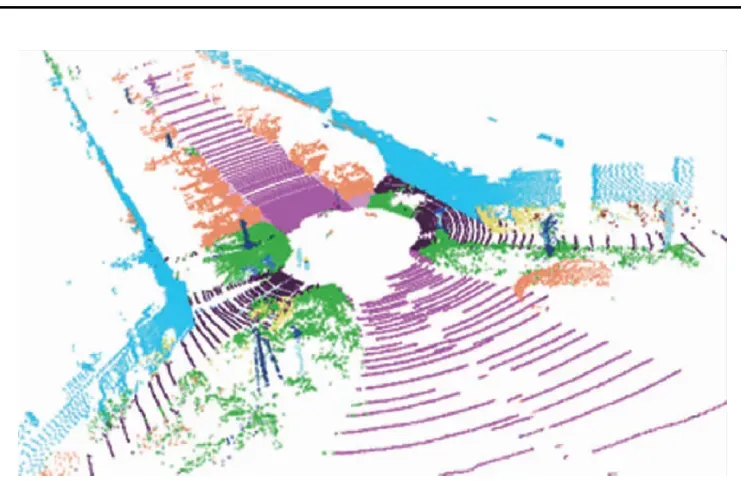
MEMS processing is based on conventional semiconductor process steps such as film deposition, photolithography, and etching.
The following sections describe several key technologies used in MEMS fabrication.
Wafers
SOI wafers
SOI stands for Silicon On Insulator and refers to a silicon wafer with a single-crystal silicon layer formed on an oxide film. SOI wafers are widely used in power devices and MEMS. In MEMS, the oxide layer can serve as an etch stop for silicon, enabling the formation of complex three-dimensional structures.
TAIKO grinding
TAIKO grinding is a technique developed by DISCO Corporation. During wafer grinding, the outermost wafer edge is preserved while grinding is applied only to the inner region. TAIKO grinding offers advantages over conventional grinding, including reduced wafer warp, higher wafer strength, easier handling, and better integration with other processes. (TAIKO is a trademark of DISCO Corporation.)
Wafer support and thermal-release film
Using a supporting wafer and a thermal-release film facilitates handling of thinned wafers during processing.
Wafer Bonding
Wafer bonding can be classified broadly into two types: direct bonding and bonding via an intermediate layer.
Direct bonding does not use adhesives. It relies on intermolecular forces generated during thermal treatment to bond wafers, and is used, for example, to produce SOI wafers. Bonding via an intermediate layer uses adhesives or other intermediate materials to join wafers.
Etching
Anisotropic and isotropic etching
Reactive ion etching generates ions and other particles in a plasma by applying a discharge under low vacuum and uses these particles for etching. The plasma contains charged ions and neutral radicals; the neutral radicals enable isotropic etching, while the ions enable anisotropic etching.
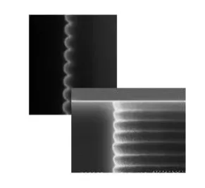
Deep silicon etching
The Bosch process, which combines the benefits of anisotropic and isotropic etching, has become the mainstream technique for deep silicon etching. By repeating cycles of silicon etching, polymer deposition, and removal of polymer from the bottom surface, vertical deep etching can be achieved. The resulting scalloped sidewall profile is referred to as a scallop morphology.
Deposition
ALD (Atomic Layer Deposition)
ALD is Atomic Layer Deposition. It deposits material one atomic layer at a time by repeating precursor exposure and purge steps, relying on surface reactions with the substrate. This method enables nanometer-scale control of film thickness and allows uniform film formation in narrow gaps, on pore sidewalls, and at the bottoms of deep holes. ALD is useful for uniform coatings in MEMS processes such as polymer deposition during deep etching.