Autonomous vehicles rely on LiDAR systems to generate precise 3D environmental maps essential for perception, path planning, and obstacle avoidance. From a PCB engineering standpoint, LiDAR modules present unique challenges: high-speed data acquisition from laser emitters and detectors, tight timing synchronization across multiple channels, robust thermal dissipation for laser diodes, and reliable interconnects for sensor fusion with cameras and other modalities. Effective PCB design directly determines the accuracy, latency, and long-term reliability of the entire perception stack.
LiDAR Operating Principles and PCB-Level Implementation
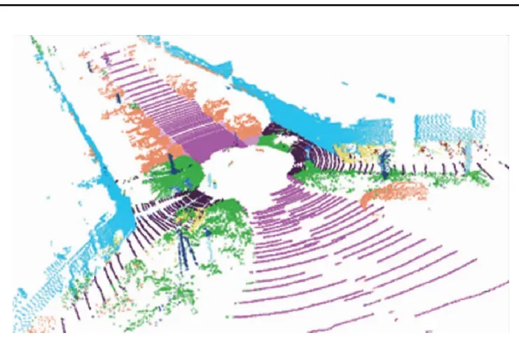
LiDAR systems measure distance by emitting laser pulses and timing their return after reflection. Single-line LiDAR uses a single rotating or oscillating beam for 2D scanning, while 3D variants employ multiple laser channels, mechanical mirrors, or solid-state arrays to generate dense point clouds. Laser triangulation methods further refine short-range measurements by calculating angles between emitter, target, and detector.
On the PCB, these principles translate into demanding layout requirements. High-frequency laser driver circuits require controlled-impedance traces, minimal via stubs, and low-inductance power delivery networks to achieve nanosecond-level pulse precision. Detector arrays (typically avalanche photodiodes or silicon photomultipliers) demand sensitive analog front-ends with excellent noise immunity. Multilayer stackups with dedicated ground planes and proper decoupling become essential to isolate high-speed digital processing from sensitive analog sections. Thermal vias and copper pours around laser diodes help manage localized heat, preventing wavelength drift that degrades ranging accuracy.
LiDAR versus Vision-Based Systems: PCB Trade-offs in ADAS Architectures
Pure vision systems use cameras for semantic understanding but struggle with depth estimation in low light or adverse weather. LiDAR provides direct, accurate distance data independent of lighting conditions. Hybrid approaches combine both for redundancy.
From the PCB perspective, LiDAR channels typically require higher bandwidth interconnects than camera interfaces. Point-cloud data streams can exceed several gigabits per second, necessitating SerDes or high-speed differential pairs with strict length matching and impedance control. Camera PCBs often prioritize MIPI CSI-2 routing and image signal processor integration. Sensor-fusion PCBs must accommodate both, using high-layer-count boards with fine-pitch routing and HDI technology to maintain signal integrity across mixed-signal domains while minimizing EMI between laser drivers and camera clocks.
3D LiDAR SLAM and Computational PCB Requirements
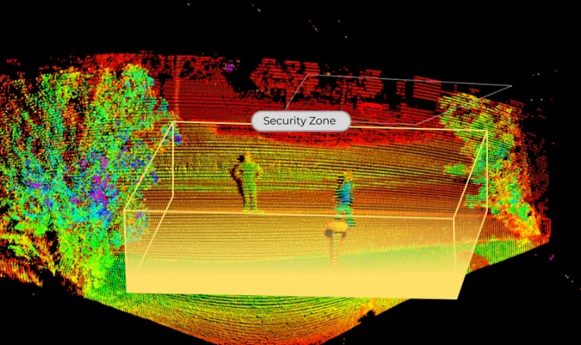
Simultaneous Localization and Mapping (SLAM) algorithms process LiDAR point clouds in real time to build maps and estimate vehicle pose. Mainstream methods include scan matching, graph-based optimization, and feature extraction.

These algorithms impose heavy computational loads that influence PCB architecture. High-performance SoCs or FPGAs handling point-cloud registration demand wide memory buses, fast DDR interfaces, and efficient power distribution. PCB designers must optimize for low-latency memory access, thermal management of dense processing packages, and robust clock distribution to maintain synchronization across LiDAR channels. Automotive-grade designs further require extended temperature materials and vibration-resistant via structures.
Sensor Fusion: Image-to-Point-Cloud Registration and Extrinsic Calibration on PCBs
Accurate fusion of 2D camera images with 3D LiDAR point clouds requires precise extrinsic calibration and temporal alignment. Asynchronous data streams must be timestamped and interpolated at the hardware level.
PCB implementation centers on high-speed communication interfaces (e.g., Ethernet, PCIe, or custom SerDes) between LiDAR and camera modules. Online extrinsic calibration routines rely on synchronized trigger signals and low-jitter clock distribution across the board. Proper grounding schemes and shielding prevent crosstalk that could corrupt calibration data. Thermal expansion differences between sensors must be accounted for in stack-up design to maintain long-term calibration stability.
Low-Light Performance and Environmental Reliability
LiDAR maintains ranging accuracy in darkness where stereo cameras lose contrast. However, both modalities benefit from careful PCB design for noise reduction and thermal stability.
Low-light camera operation increases image sensor gain, amplifying noise that fusion algorithms must filter. LiDAR benefits from high-sensitivity detectors but requires clean analog power rails. Automotive PCBs must withstand wide temperature swings, humidity, and vibration. High-Tg laminates, thick copper for power planes, and conformal coating options improve reliability. Signal integrity simulations covering temperature and aging effects help ensure consistent performance.
Pedestrian Re-Identification and Edge Processing Considerations
LiDAR-based pedestrian re-identification leverages point-cloud shape and motion features, often fused with visual data for higher accuracy. Real-time processing on the vehicle demands efficient edge computing.
PCB designs supporting these tasks incorporate powerful neural-network accelerators with high-bandwidth memory interfaces. Power integrity becomes critical during peak inference loads. Compact module footprints favor HDI and microvia technology, while thermal management solutions (heat sinks, thermal interface materials) keep junction temperatures within limits for sustained reliability.
Future Trends and PCB Manufacturing Implications
Solid-state LiDAR, higher channel counts, and tighter integration with domain controllers continue to push PCB requirements toward finer features, advanced materials, and 3D packaging compatibility. Increased data rates drive adoption of low-loss dielectrics and optimized stack-ups. Automotive qualification (AEC-Q200, ISO 26262 functional safety) adds layers of validation for via reliability, thermal cycling performance, and EMI compliance.
Early collaboration between LiDAR system architects and PCB manufacturers enables optimized stack-up definition, material selection, and manufacturing processes that balance performance, yield, and cost. Techniques such as back-drilling, filled vias, and precise impedance control directly support the stringent timing and signal-quality demands of next-generation autonomous perception systems.
Conclusion
Effective LiDAR integration in autonomous vehicles ultimately hinges on PCB-level engineering decisions that balance extreme bandwidth, nanosecond-level timing precision, thermal management, and sensor-fusion synchronization against the realities of layout constraints, signal integrity, and automotive-grade reliability. As solid-state architectures and higher channel counts accelerate, early collaboration between perception system designers and PCB manufacturing specialists becomes indispensable to avoid costly iterations and ensure consistent performance across temperature extremes, vibration, and long service life. By applying rigorous stack-up optimization, controlled-impedance routing, advanced via technologies, and comprehensive validation processes, engineering teams can deliver perception hardware that meets the stringent demands of safe, scalable autonomous driving. Aivon’s expertise in high-performance, automotive-qualified PCB fabrication equips partners to navigate these complexities with confidence, producing boards that fully unlock the potential of next-generation LiDAR systems.