Overview
Thermal emission spectra are widely used in environmental monitoring, astrophysics, medical diagnostics, and drug development. Infrared emitters based on microelectromechanical systems (MEMS) have effectively reduced device size, but they often exhibit broad spectral distributions and low emissivity. By engineering micro- and nano-scale structures, it is possible to control the spectral characteristics of thermal emission and realize narrowband emission with improved performance.
According to MEMS Consulting, a research team from the Yangtze River Delta Research Institute and the School of Optoelectronic Science and Engineering at the University of Electronic Science and Technology of China recently published an article titled "MEMS Narrowband Infrared Thermal Emitters Based on Micro-nano Structures and Their Applications" in Progress in Laser and Optoelectronics. The first author is Li Ruoyu and the corresponding author is Guo Xiaowei.
This article summarizes the operating principles of MEMS thermal infrared sources, reviews progress on narrowband infrared sources realized with different micro-nano structures, and discusses applications in gas sensing, thermophotovoltaic power generation, and biomedical imaging.
Principle of MEMS Thermal Infrared Sources
A common MEMS infrared emitter uses a suspended resistive heater structure. The base is a silicon substrate, above which a supporting layer and heating resistor are deposited, and a patterned micro-nano layer can be added to the surface. The supporting layer is often a composite of SiO2 and Si3N4: SiO2 provides compressive stress and good thermal isolation, while Si3N4 supplies tensile stress and high mechanical strength. The composite balances residual stress in the films, reduces deformation at high temperature, and stabilizes long-term performance. Heating resistors are typically made of polysilicon or metal to ensure stable resistance at elevated temperatures.
MEMS thermal infrared emitters generate infrared radiation by resistive (Joule) heating. Under an applied voltage, the heater produces thermal radiation, and the energy in the radiating region propagates via three paths governed by energy conservation: radiative emission from the radiating region, convective loss to the surrounding air, and conductive heat transfer through the supporting layer to the silicon substrate.
One approach to increase absorption is to use inherently high-absorptivity materials such as black silicon or copper manganese oxides, but these materials do not allow precise control of emission wavelength and bandwidth. An alternative is to use optical micro- and nano-structures to enhance light–matter interaction at specific wavelengths. By designing structural dimensions, resonant wavelengths with near-perfect absorption can be achieved, producing strong narrowband emission.
Narrowband Emitters Based on Micro-nano Structures
Photonic Crystals
Photonic crystals are materials with periodic variations in refractive index or dielectric constant. The periodic geometry produces unique optical transmission phenomena. Photonic crystal periodicity can interact with surface plasmon or phonon resonances on metal or polar material films, enhancing emission at specific wavelengths. By tuning photonic crystal parameters, the resonance frequency can be controlled to create narrowband infrared emitters targeted to specific bands.
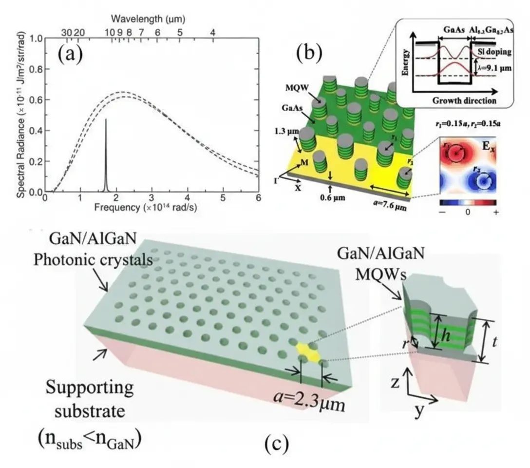
Using this concept, M. U. Pralle et al. (2002) coated a metal film on a silicon square-lattice photonic crystal to excite surface plasmon modes and achieved δλ/λ ≤ 0.2 narrowband infrared emission with over 90% absorption within the narrow band. Later work demonstrated that changing lattice dimensions in two-dimensional photonic crystals allows flexible tuning of the emission band, as shown in Figure 3.
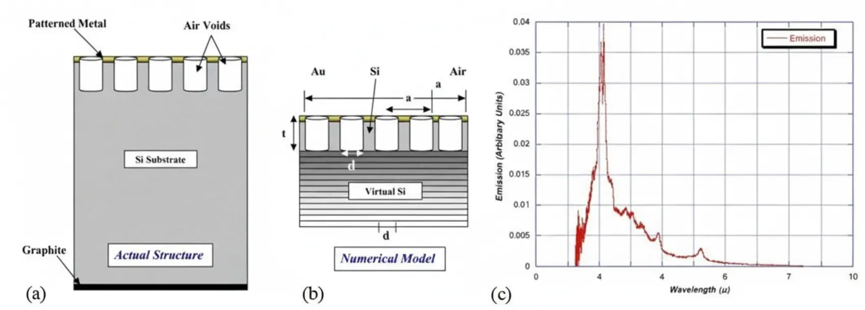
Figure 1: (a) Cross-section of a photonic-crystal based narrowband emitter; (b) numerical modeling; (c) emission spectrum.
Other groups have fabricated high-performance plasmonic thermal emitters by depositing platinum on periodically patterned silicon photonic crystal substrates, enabling spectral tuning via lattice constant control. A separate approach combined semiconductor quantum wells with a two-dimensional photonic crystal cavity to produce narrow, strong thermal emission. One design showed radiation intensity reaching 80% of blackbody at a center wavelength near 11 μm with FWHM ≈ 0.11 μm at 600 K.
Gratings
Gratings are another common micro-nano structure used to tailor surface emissivity for monochromatic and directional emission. Gratings couple thermally generated surface waves into free space. Polar materials (e.g., SiC, GaP) can excite surface phonon polaritons (SPhP), while metals support surface plasmon polaritons (SPP). Momentum mismatch between incident light and SPhP/SPP can be compensated by patterned surface gratings.
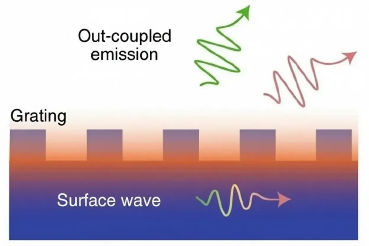
Figure 3: Grating coupling of thermal surface waves into free space.
Examples include subwavelength gratings etched on Au surfaces to achieve linearly polarized narrowband thermal emission based on SPPs, and silicon-based gratings coated with metal films to create narrowband emitters. Some structures extend gratings into two dimensions to enable coherent thermal emission for both TE and TM polarizations, such as SiC cross-slot grating structures.
Recent work has exploited quasi-bound states in the continuum (QBIC) in staggered grating waveguide structures to realize ultra-narrowband mid-infrared thermal emitters. Another approach uses plasmonic stacked gratings where a two-dimensional metal nanostructure array sits atop a Bragg grating, producing emission resonances inside the Bragg gap and reducing FWHM below 0.1 μm through bandgap engineering.
Metasurfaces
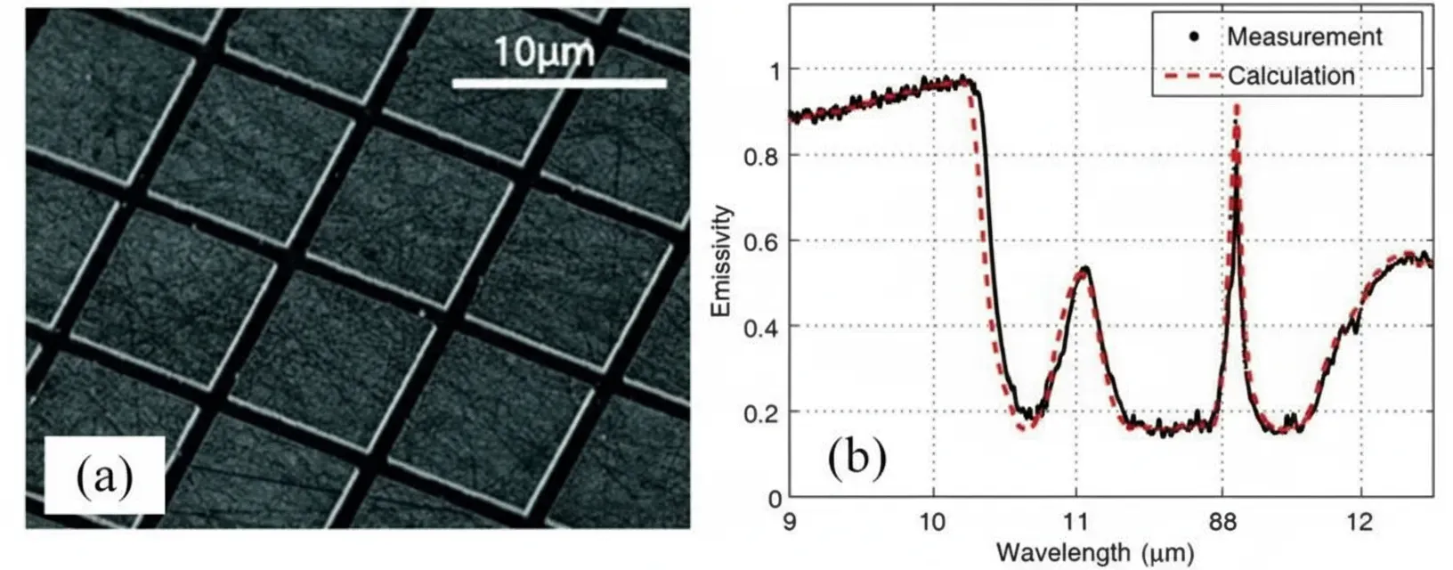
Metasurfaces are planar metamaterials that provide nonconventional control over light and thermal radiation. Most metasurface thermal emitters use metal-insulator-metal (MIM) configurations, where a periodic array of thin metal elements produces electromagnetic resonances in the infrared. Resonant wavelengths are selectively emitted while other bands are not, enabling wavelength-selective emission. Metasurface emitters can demonstrate multi-band, polarization-dependent or polarization-insensitive, directional, and near-perfect emission characteristics not available in traditional materials.
Examples include TiN/SiO2/TiN trilayer narrowband infrared emitters where surface pattern period and size control emission wavelength; devices with two-band, polarization- and angle-insensitive emission; and on-chip narrowband emitters based on metamaterials. All-dielectric metasurfaces on conductive substrates have also been shown to support QBIC modes for ultra-narrowband mid-infrared thermal emission.
Applications of Narrowband Infrared Emitters
Gas Sensing Sources
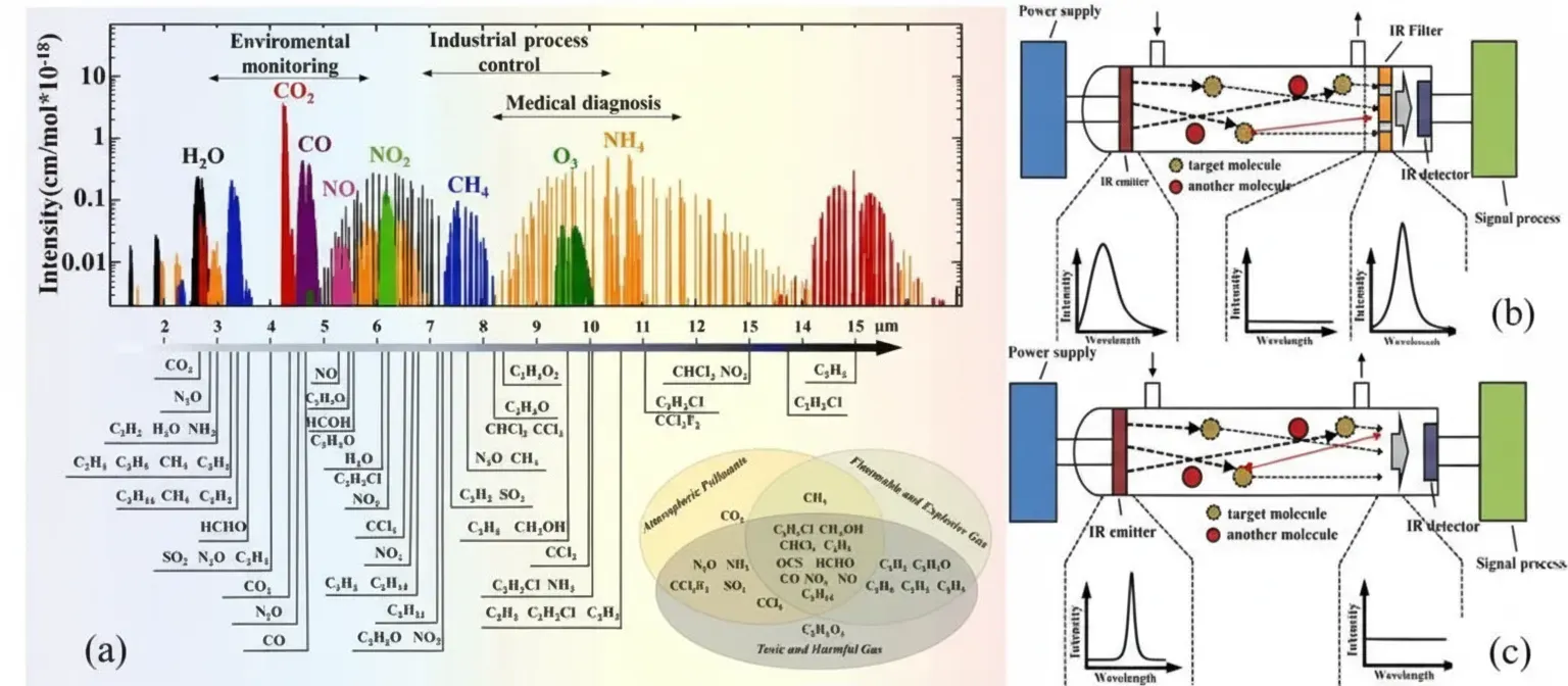
Gases such as CO2, CO, and CH4 interact with infrared light at characteristic wavelengths due to changes in molecular dipole moments. Each gas has absorption resonances at specific wavelengths; different concentrations change the amount of absorbed infrared energy. Narrowband infrared emitters concentrate energy near target gas absorption wavelengths, improving sensitivity and accuracy compared with broadband sources. Figures below summarize common gas absorption spectra from 2 to 15 μm and compare conventional broadband detection with narrowband source approaches, showing higher energy efficiency and simplified system design when using narrowband emitters.
Thermophotovoltaic Power Generation
Near-infrared and visible thermal emission can be converted to electricity by photovoltaic (PV) cells in thermophotovoltaic (TPV) systems. Emission outside the PV cell bandgap is not absorbed and lowers conversion efficiency. High-performance TPV systems require spectral matching between thermal emission and the PV cell spectral response. Narrowband thermal emitters that concentrate emissivity within the PV-sensitive region while suppressing emission outside that band can improve TPV efficiency. For example, a tungsten grating heated to emit in the 1.6–1.9 μm band has been used to couple thermal emission to PV cells for TPV demonstration.
Biomedical Imaging and Stimulation
Mid-infrared imaging is a reliable tool for studying tissue sections and cell cultures. Unlike visible microscopy that often requires staining, mid-infrared imaging can provide label-free molecular information from tissue samples. Narrowband infrared thermal emitters combined with spectroscopic analysis enable noninvasive detection and imaging of internal tissues and organs, supporting early cancer diagnosis and intraoperative margin assessment via mid-infrared endoscopic spectral imaging.
Narrowband infrared emitters can also provide illumination or stimulation in cell culture experiments. Targeted infrared irradiation helps study cell behavior or activate light-sensitive agents. Infrared light has photobiomodulation effects useful in neural modulation, wound healing, and cancer therapy.

Summary
Periodic micro- and nano-scale structures enable control of thermal emission spectra through optical resonances. Research on MEMS narrowband infrared thermal emitters is important for improving spectral resolution, enhancing biomedical imaging performance, and advancing infrared materials and devices. By selecting appropriate nanostructure types, thermal emission can be tailored from single-peak to multi-band, polarization-sensitive or polarization-insensitive, and across wavelengths from near- to mid-infrared.
Photonic crystal and grating based emitters typically achieve stronger narrowband emission with smaller FWHM than many metasurface implementations. However, those structures are sensitive to temperature and require high fabrication precision, where small deviations can shift emission peak position and width. Metasurface emitters often use MIM stacks; metal losses can produce unwanted nonzero emission outside resonances and broaden resonance peaks, increasing FWHM. To reduce metal loss, researchers are exploring low-loss metals and dielectric alternatives to improve metasurface narrowband performance and reduce FWHM.
Future MEMS narrowband infrared source development will focus on improving source efficiency, enhancing structural and performance stability, further reducing device size and cost, and achieving more precise and stable narrowband emission. MEMS infrared narrowband thermal emitters are compatible with standard CMOS materials and processes, enabling on-chip integration and combination with other sensors or devices for advanced imaging and sensing applications.