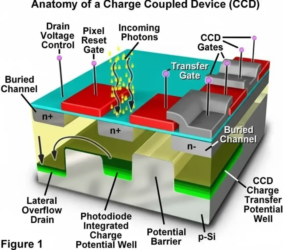
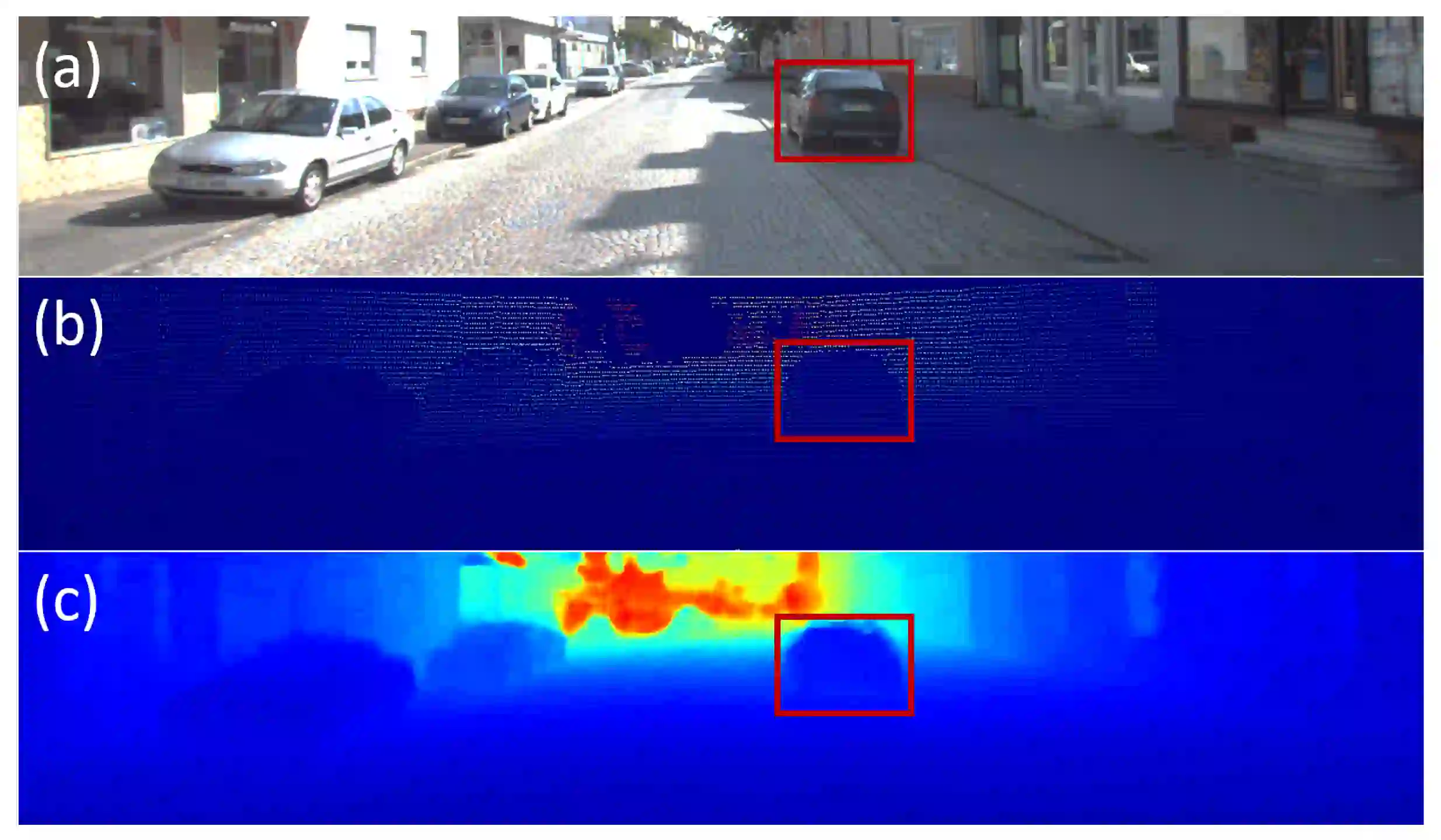
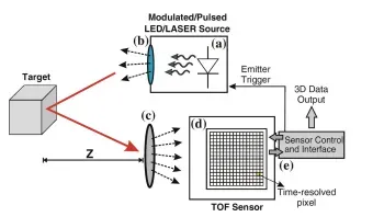
Help
  • FAQ
    browse most common questions
  • Live Chat
    talk with our online service
  • Email
    contact your dedicated sales:
0

Nanoscale Structures Reshape Miniature Cameras and Projectors

Author : AIVON | PCB Manufacturing & Supply Chain Specialists March 16, 2026


Overview

Ultra-thin semiconductor lenses are finally reaching consumer devices.

In today’s computers, phones, and other mobile devices, growing numbers of sensors, processors, and other electronics compete for space. Cameras occupy a large portion of this valuable space: almost every device needs one or two, sometimes more. The lenses account for much of a camera’s volume.


Limits of Conventional Refractive Lenses

Mobile device lenses typically collect and direct incoming light by refraction, using curved transparent materials, usually plastic, to bend the rays. Those lenses cannot be scaled down indefinitely: making a compact camera requires a short focal length; the shorter the focal length, the greater the curvature and the thicker the lens center. Highly curved lenses also introduce various aberrations, so camera module makers stack multiple lens elements to compensate, increasing module thickness.

Today, image quality and camera size push in opposite directions. The only way to make lenses both smaller and better is to replace refractive elements with a different technology.


Metalenses: Flat Optics Built with Nanostructures

This alternative exists. Known as the metalens, the device was developed at Harvard University and commercialized by Metalenz. Using standard semiconductor fabrication techniques, nanostructures are patterned on a flat plane to form the lens. These nanoscale elements exploit a phenomenon called metasurface optics to steer and focus light. Metalenses can be extremely thin, only a few hundred micrometers thick, roughly twice the diameter of a human hair. They can combine the functions of multiple curved lenses into a single element, addressing space constraints and opening new possibilities for imaging in mobile devices.


Historical Context and Alternative Approaches

Any device that manipulates light does so by changing the three fundamental properties of a wave: phase, polarization, and amplitude. This idea dates back to Christian Huygens in 1678 and remains a guiding principle in optics.

In the early 18th century, lighthouse beams demanded ever larger projection lenses. As these lenses grew, so did their weight, and physical size limited how powerful lighthouse beams could be. Augustin-Jean Fresnel observed that slicing a lens into concentric flat sections could remove much of the center thickness while preserving optical power. Fresnel lenses represent a major optical advance and are used in headlamps, overhead projectors, and lighthouses. However, Fresnel lenses have limits: the edges of the flat segments cause stray light, and segmented surfaces are harder to manufacture and polish to the precision required for high-quality camera images.

Another approach widely used in 3D sensing and machine vision traces back to Thomas Young’s 1802 diffraction experiments, which demonstrated light’s wave properties and interference. Diffractive optical elements, or DOEs, use interference patterns to create arrays of bright and dark regions that can form point patterns, grids, or other shapes. Many mobile devices use DOEs to convert a laser into structured light patterns for 3D mapping. DOEs are well suited to small devices but cannot produce high-fidelity images, so their applications remain limited.


How Metalenses Work

Metalenses, developed in Federico Capasso’s lab at Harvard with contributors such as Rob Devlin, Reza Khorasaninejad, and Wei Ting Chen, operate on a fundamentally different principle. A metalens is a flat glass surface coated with a semiconductor layer, on which rows of pillars hundreds of nanometers high are etched. These nanopillars manipulate light waves at a level not possible with traditional refractive lenses.

Imagine a shallow marsh of tall grasses. When waves pass, the grass stalks sway and alter the wave pattern. If incident waves represent light and the nanopillars represent grass stalks, you can visualize how the nanopillar properties—height, diameter, and spacing—change the distribution of light transmitting through the lens.

Using a metalens, light can be scattered or projected as an infrared dot field; many smart devices use invisible dot patterns to measure distance, map rooms, or capture facial geometry. Metalenses can also sort light by polarization. To explain imaging with these metasurfaces, consider capturing an image with monochromatic illumination, such as a laser. Light reflecting from objects in the scene returns to the metalens, where photons interact with the nanopillar tops and convert into oscillations called plasmons that propagate along the pillars. When energy reaches the pillar base, it re-emerges as photons that the image sensor can detect. The properties of these outgoing photons can differ from the incoming ones; designers control those properties by adjusting the nanopillar geometry and layout.


Research and Development

Researchers worldwide have studied metasurfaces for decades. In 1968 Victor Veselago introduced the concept of metamaterials and the possibility of materials with a negative refractive index. That idea matured experimentally around 2000, when groups demonstrated negative-index materials in the microwave band, generating wide interest in novel optical applications.

Capasso’s lab produced the first metalenses capable of forming high-quality images in the visible range. A 2016 Science paper describing the technology attracted attention from smartphone manufacturers. Harvard licensed the foundational intellectual property to Metalenz, which has pursued commercialization. Subsequent work at Columbia University, Caltech, and the University of Washington with collaborators including Tsinghua University has also advanced the field.

Metalenz’s development work has focused on precise device design. To translate image characteristics such as resolution into nanoscale patterns, the team developed tools that compute how light waves interact with materials, then convert those computations into design files usable by standard semiconductor fabrication equipment.

Early optical metasurfaces incorporated tens of millions of silicon pillars on a single plane of only a few square millimeters. Each pillar must be tuned to impart the correct optical phase, and even with advanced software, this design process is complex. Next-generation metalenses may not require more pillars, but pillar geometries could become more complex, for example with tilted edges or asymmetric shapes.


Manufacturing Advantages

In 2021 Metalenz announced plans to scale production. Manufacturing challenges are typically less severe than design challenges because metasurfaces use the same materials, photolithography, and etching processes as integrated circuit manufacturing.

In fact, producing metalenses can be simpler than fabricating many microchips, since metalenses may require only a single photomask while processors need dozens. That reduces defect likelihood and cost. Also, optical metasurfaces have feature sizes on the order of hundreds of nanometers, while foundries regularly fabricate chips with feature sizes below 10 nanometers.

Unlike plastic lenses, metalenses can be manufactured in the same foundries that produce other smartphone chips. That enables on-site integration with complementary metal-oxide-semiconductor, or CMOS, camera chips without shipping elements between suppliers, further lowering cost.


Early Commercial Use and Sensing Applications

In 2022 STMicroelectronics announced integration of Metalenz’s metasurface technology into its FlightSense module. Previous FlightSense generations have been used in over 150 models of smartphones, drones, robots, and vehicles for distance sensing. Products using Metalenz technology have reached consumers, though STMicroelectronics did not disclose detailed specifications.

The most prominent effect of the current generation of metalenses, which operate at near-infrared wavelengths, is distance sensing. Many consumer electronics companies use time-of-flight systems with two optical subsystems: one to emit light and another to receive it. The emitter optics are more complex, requiring multiple lenses to collimate laser light and a diffractive grating to create a dot-field. A single metalens can replace all emitter and receiver optics, saving space and reducing cost.

Under poor lighting, metalenses perform well in dot-field generation because they can illuminate large areas with less energy than traditional lenses, directing more light to desired regions.


Polarization Imaging and New Capabilities

Conventional imaging systems collect information about object position, color, and brightness. Light also carries information about propagation direction, known as polarization. Future metalens applications will exploit this capability to detect polarization directly.

The polarization of reflected light reveals object properties such as surface texture, material type, and penetration depth before reflection. Before metalenses, machine vision systems needed complex mechanical subsystems to gather polarization data, typically using a rotating polarizer in front of the sensor. The polarizer acts like a fence allowing only waves oriented at specific angles to pass; the system records how the detected light intensity changes with rotation angle.

Metalenses can route all incoming light without a physical grid. A single optical element can direct light to specific sensor regions based on polarization. For example, light polarized along the x axis might be guided to one sensor area, while light polarized at 45 degrees is guided elsewhere. Software can then reconstruct an image with full polarization-state information.

This approach enables miniaturized polarization analyzers integrated in smartphones, vehicles, or augmented-reality glasses that could replace expensive laboratory equipment. Potential use cases include distinguishing diamonds from glass, assessing concrete curing, evaluating the condition of a hockey stick, detecting small cracks, monitoring bridge supports, identifying whether road patches are black ice or water, and discriminating painted surfaces from vegetation. Polarization sensing can also aid anti-spoofing in facial recognition, since reflections from a 2D photo differ from those of a 3D face, and reflections from a silicone mask differ from skin. Handheld polarization devices could also support remote medical diagnosis, for example by helping to detect tissue abnormalities.


Outlook

As with smartphones themselves, it is difficult to predict all applications that metalenses will enable. When Apple introduced the iPhone in 2008, its broader ecosystem could not have been predicted. Similarly, the most exciting metalens applications may be those we cannot yet imagine.

metalens nanostructure concept

AIVON | PCB Manufacturing & Supply Chain Specialists AIVON | PCB Manufacturing & Supply Chain Specialists

The AIVON Engineering and Operations Team consists of experienced engineers and specialists in PCB manufacturing and supply chain management. They review content related to PCB ordering processes, cost control, lead time planning, and production workflows. Based on real project experience, the team provides practical insights to help customers optimize manufacturing decisions and navigate the full PCB production lifecycle efficiently.

Related Tags


2026 AIVON.COM All Rights Reserved
Intellectual Property Rights | Terms of Service | Privacy Policy | Refund Policy