CMOS image sensors have dominated consumer and industrial imaging since the early 2000s by enabling compact, cost-effective camera modules. However, conventional silicon-based detectors exhibit saturation in highlights, elevated noise in low light, limited color fidelity, and transparency beyond approximately 1 µm wavelength, restricting near-infrared performance. These constraints motivate exploration of alternative absorber materials such as quantum dots.
Quantum Dot Fundamentals and Tunable Properties
Quantum dots are semiconductor nanocrystals a few nanometers in diameter. Quantum confinement confines charge carriers, enabling precise tuning of absorption and emission wavelengths through material composition and particle size. This tunability spans visible and short-wave infrared (SWIR) bands. Quantum dots can be formulated as printable inks, allowing deposition via spin-coating or inkjet processes onto existing silicon readout circuits. Their high absorption coefficient supports thinner active layers compared with silicon, potentially improving dynamic range and reducing overall stack height.
Comparison of Operating Principles
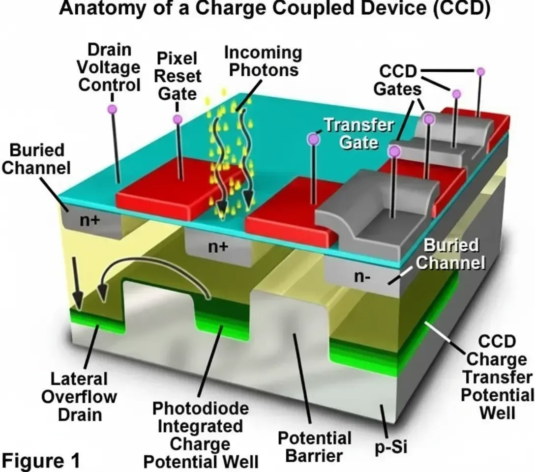
In a standard CMOS sensor, light passes through color filters onto silicon photodiodes. Photogenerated electrons are collected and read out through integrated circuitry. Front-illuminated designs suffer reflection losses from overlying metal layers, while back-illuminated architectures require complex wafer thinning and bonding steps. Silicon’s bandgap prevents efficient detection beyond ~1 µm.
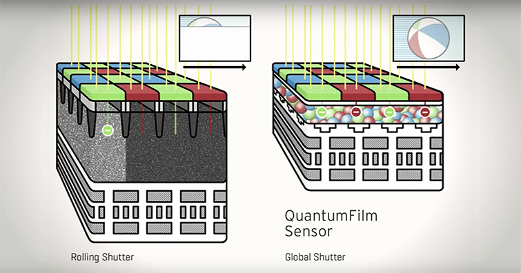
Quantum dot detectors replace the silicon absorber with a thin film of nanocrystals deposited atop a conventional silicon readout integrated circuit (ROIC). Photons absorbed by the quantum dots release electrons that hop between adjacent dots to reach pixel electrodes. Readout circuitry remains fabricated using standard CMOS processes, while the quantum dot layer is added through a comparatively simple coating step. This architecture inherently supports back-illumination without additional wafer-level processing, and the thin absorber layer captures most incident photons within a reduced thickness.
Infrared Imaging Advantages and Hybridization Elimination
Quantum dots can be synthesized for SWIR sensitivity using materials such as lead sulfide. Traditional SWIR detectors based on indium gallium arsenide or mercury cadmium telluride are fabricated separately and hybridized to silicon ROICs via indium bump bonding. This hybridization limits pixel pitch (typically ≥15 µm), reduces throughput, and increases cost. Quantum dot layers applied directly onto completed ROICs eliminate the bonding step, enabling smaller pixels, higher resolution arrays, and reduced sensor size. Smaller focal-plane arrays in turn allow more compact and lower-cost optics.

Key Technical Challenges
Stability remains a primary concern. Quantum dots are susceptible to oxidation in ambient air, leading to degraded sensitivity, increased noise, and potential electrical shorts. Encapsulation strategies must permit charge transport while protecting the film. Organic ligands used for colloidal stability can impede conductivity; ligand-exchange processes improve transport but may introduce surface defects and long-term degradation.
Efficiency is another limitation. Reported external quantum efficiencies for quantum dot photodetectors are often below 20 %, compared with >50 % for single-crystal semiconductor detectors, due to surface defects and non-radiative recombination. Ongoing material and device engineering aim to close this gap. Uniformity is affected by inherent size variation in chemical synthesis, requiring tight process control during purification and deposition to maintain consistent pixel response across large arrays.
Applications and System-Level Considerations
Quantum dot sensors target applications where cost-effective SWIR imaging provides value, including industrial inspection, maritime surveillance, automotive night vision, and enhanced smartphone features such as improved low-light photography and facial recognition. In consumer devices, integration with existing CMOS readout and processing pipelines reduces development overhead. In industrial systems, higher-resolution SWIR arrays at lower cost enable broader deployment of spectral imaging for material identification and process monitoring.
Design Constraints and Manufacturing Implications
Integration of quantum dot layers onto silicon ROICs imposes requirements on surface cleanliness, adhesion, and thermal budget during deposition. The thin absorber must maintain electrical contact with pixel electrodes while minimizing leakage paths. Readout circuitry must accommodate potentially different charge-generation and recombination dynamics compared with silicon photodiodes, affecting pixel architecture, gain settings, and noise performance.
Scalability challenges include maintaining batch-to-batch consistency of quantum dot size distribution and film morphology across wafer-scale or panel-scale processing. Yield depends on defect density in the deposited layer and compatibility with subsequent packaging steps. Reliability testing must address accelerated aging under humidity, temperature cycling, and illumination stress to verify long-term stability of both the quantum dot film and its interface with the ROIC.
PCB Layout, Materials, and Electronic Integration
Image sensor modules interface with host systems through high-speed serial links (MIPI CSI-2, LVDS) that demand controlled-impedance transmission lines and low-noise power delivery. PCB stackup design must isolate sensitive analog sensor supplies from digital switching noise while providing adequate thermal paths for heat generated by the sensor and downstream processors. Low-loss laminates and precise copper thickness control support signal integrity at multi-gigabit data rates. Thermal vias and copper balancing help maintain stable operating temperatures that minimize dark current and offset drift.
Suggested Reading: Understanding CIS Camera Chips and Image Sensors
Flexible printed circuits (FPCs) enable compact camera modules in mobile or wearable devices, requiring polyimide substrates with appropriate dimensional stability and low outgassing. High-density interconnect (HDI) technology supports fine-pitch interconnects between the sensor package and surrounding circuitry. Material selection for underfill, encapsulation, and optical windows must balance optical transmission, mechanical protection, and thermal expansion matching to prevent stress on the sensor die or quantum dot layer.
Manufacturing processes for the complete module include precise die attach, wire bonding or flip-chip attachment, and optical alignment. Electrical testing verifies continuity, noise performance, and quantum efficiency after assembly. Reliability qualification encompasses thermal shock, vibration, and humidity exposure to ensure consistent image quality over the product lifetime.
Industry Trends
Research institutions and companies continue to improve quantum dot stability through surface passivation and encapsulation techniques while raising device-level efficiency. Integration with advanced CMOS nodes and on-chip signal processing supports higher frame rates and lower power consumption. Regulatory and supply-chain considerations for novel materials influence adoption timelines in consumer and automotive markets.
Electronic Manufacturing and PCB Technologies Supporting Quantum Dot Sensor Systems
Quantum dot image sensor modules depend on multilayer PCBs with controlled-impedance routing and mixed-signal partitioning to preserve low-noise performance from the sensor through the digital interface. Fabrication processes that deliver consistent dielectric properties and fine-feature copper traces enable reliable high-speed data transmission. Assembly techniques, including precise sensor placement, thermal management solutions, and robust encapsulation, support the transition from prototype to volume production while maintaining optical and electrical performance. These manufacturing considerations directly influence image quality, system power consumption, and long-term reliability in automotive, industrial, and consumer imaging applications.
Conclusion
Quantum dot image sensors provide tunable spectral response and simplified fabrication paths that address specific limitations of conventional CMOS detectors, particularly in the short-wave infrared. Realizing these benefits at scale requires coordinated advances in material synthesis, device architecture, and electronic system integration. Printed circuit board technologies play an essential role by ensuring signal integrity, thermal stability, and mechanical reliability of the complete imaging module.