Overview
Detecting hidden structures or defects in materials is important in engineering and materials science. Conventional terahertz imaging systems exploit terahertz waves' ability to penetrate optically opaque materials and have been developed to reveal internal structures of interest. These capabilities are useful in industrial quality control, security screening, biomedical applications, and defense. However, most existing terahertz imaging systems have limited throughput, require bulky setups, and rely on raster scanning to form images of hidden features.
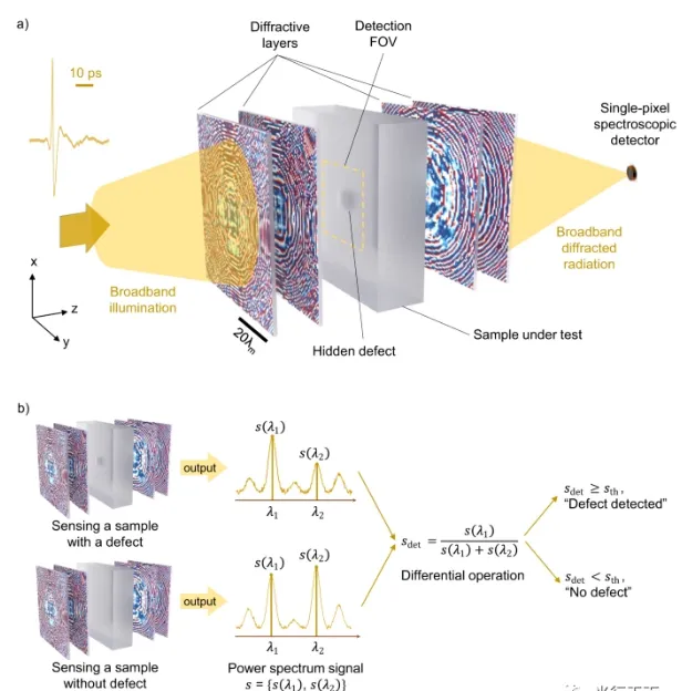
Figure: Schematic of a diffractive terahertz sensor using a single-pixel spectral detector to rapidly detect hidden objects or defects.
Single-Pixel Diffractive Sensor Concept
To change this paradigm, researchers at the Samueli School of Engineering and the California NanoSystems Institute at the University of California, Los Angeles developed a terahertz sensor that can rapidly detect hidden defects or objects within a sample volume using a single-pixel spectral terahertz detector.
Unlike point-by-point scanning and digital image-formation approaches, the sensor illuminates the sample volume once with terahertz radiation and does not require image formation or digital processing of the sample.
Design and Operation
The sensor, led by Dr. Aydogan Ozcan, chair of the Department of Electrical and Computer Engineering at UCLA, and Dr. Mona Jarrahi, Northrop Grumman Professor, functions as an all-optical processor that is designed to search for and classify unexpected wave sources produced by diffraction from hidden defects. The research was published in Nature Communications.
Dr. Ozcan said, "As we move away from traditional methods toward more efficient, AI-driven all-optical sensing systems, our perspectives and uses of terahertz imaging and sensing have shifted."
The diffractive terahertz sensor consists of a series of diffractive layers that are automatically optimized using deep learning algorithms. After training, these layers are converted into physical prototypes using additive manufacturing methods such as 3D printing. This enables the system to perform all-optical processing without the need for raster scanning or digital image capture and processing.
Dr. Ozcan compared the approach to previous AI-designed optical neural networks: the design includes multiple diffractive layers that modify the input terahertz spectrum depending on whether hidden structures or defects are present in the test material. Conceptually, the sensor perceives and responds in real time to what it 'sees' at the speed of light.
Experimental Validation
To demonstrate the concept, the UCLA team 3D-printed a diffractive terahertz sensor and successfully detected hidden defects in silicon samples. The samples were composed of stacked wafers where one layer contained a defect that was concealed by another layer. The trained system accurately revealed the presence of unknown hidden defects with various shapes and positions. The researchers believe the diffractive defect-sensing framework can be applied at other wavelengths, such as infrared and X-ray.
Applications and Advantages
The method's non-imaging simplicity, high throughput, and cost-effectiveness point to applications ranging from manufacturing quality control and security screening to cultural heritage preservation. The approach may offer improvements in speed, efficiency, and accuracy for applications where those factors are critical.