Residual stress is a primary concern in MEMS development because it directly influences device performance, mechanical integrity, and long-term reliability. Stresses are classified by origin into intrinsic (internal) stress and thermal mismatch stress. Intrinsic stress develops during film deposition from lattice mismatch and process parameters. Thermal mismatch stress arises from differences in coefficients of thermal expansion (CTE) between layers when temperature changes occur. Both types must be understood and controlled to prevent wafer warpage, film delamination, cracking, or functional failure in suspended structures such as membranes and cantilevers.
Intrinsic Stress in Thin Films
Intrinsic stress, also termed internal stress, exists within a material at room temperature in the absence of external loads. It can be tensile or compressive and is especially critical in MEMS thin films. Non-uniform stress through the film thickness creates a stress gradient. When this gradient exceeds the film's elastic modulus, the film deforms, leading to wafer bow, delamination, or cracking.
Composite film stacks used in many MEMS structures require careful balancing of stresses between layers. Intrinsic stress originates primarily during deposition; key influencing factors include method (evaporation versus magnetron sputtering), temperature, pressure, and deposition rate. For example, evaporated gold films typically exhibit lower intrinsic stress than sputtered films.
Low-pressure chemical vapor deposition (LPCVD) of silicon nitride (SiNₓ) illustrates process control requirements. Achieving low-stress films generally demands silicon-rich conditions through elevated DCS/NH₃ ratios, together with precise management of temperature, pressure, and reaction time. Temperature gradients along the furnace tube can cause significant wafer-to-wafer stress variation; raising the center-zone temperature helps minimize these differences.
Thermal Mismatch Stress
Thermal mismatch (or thermal) stress occurs at interfaces between materials with differing CTEs when temperature changes. Two conditions are required: dissimilar CTE values and a temperature excursion. This stress is inherent to MEMS fabrication sequences and operational environments. Non-elastic (plastic) deformation induced by thermal stress can cause process failures or reliability degradation. Consequently, thermal budgets are progressively tightened, with high-temperature steps restricted to early process stages whenever possible.
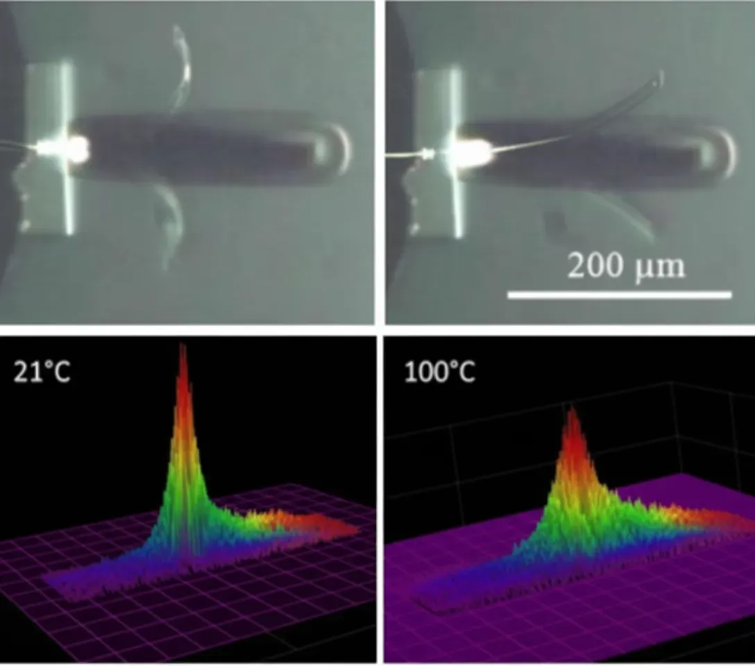
Thermal mismatch can be intentionally exploited. Bilayer thermal actuators rely on CTE differences to produce controlled bending: temperature rise deflects the cantilever toward the lower-CTE layer, with return to the neutral position upon cooling.
Achieving Stress Matching in Multilayer Structures
Stress matching is essential in MEMS process design. Without balanced film stresses, devices are prone to immediate or latent failure. Practical methods are illustrated using chromium (Cr) and gold (Au) films for metal cantilevers. Typical magnetron-sputtered values are Cr intrinsic stress ≈ 1000 MPa and CTE ≈ 4.9 × 10⁻⁶/°C; Au intrinsic stress ≈ 200 MPa and CTE ≈ 14.1 × 10⁻⁶/°C.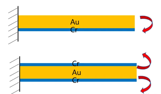
Two-Layer Composite Films
With Cr as the bottom layer and Au on top, both intrinsic stress gradient and thermal mismatch drive downward bending (toward higher-stress/lower-CTE Cr). In practice, Cr serves as an adhesion layer; solutions include minimizing Cr thickness and intrinsic stress while increasing Au thickness to counteract deformation.
Three-Layer (Sandwich) Composite Films
A Cr/Au/Cr stack enables mutual compensation. Intrinsic stress gradients allow the central Cr layer to bend toward both Au layers, while the lower CTE of Cr similarly compensates thermal stress. Equal top and bottom layer thicknesses are required for simultaneous intrinsic and thermal balancing.
Odd-numbered layer counts generally outperform even-numbered configurations for stress compensation. The design priority is first to minimize intrinsic stress in each individual layer through deposition optimization; once low-stress films are achieved, inter-layer compensation becomes the decisive factor for successful device fabrication.
Manufacturing and Reliability Considerations
Stress matching directly impacts yield, process scalability, and device lifetime. Non-uniform stress leads to wafer-level warpage that complicates lithography alignment and subsequent handling. Excessive gradients cause delamination during release steps or thermal cycling in operation. Process engineers therefore combine deposition-parameter tuning, layer-thickness optimization, and symmetric stack designs. Post-deposition annealing or stress-relief steps may be introduced, subject to thermal-budget constraints.
Testing typically includes wafer bow measurements, cantilever deflection metrology, and accelerated thermal cycling to validate stress compensation. Material selection must also consider long-term stability, electromigration in metal films, and compatibility with release etches.
Relevance to Electronics Manufacturing and PCB/FPC Integration
MEMS devices are frequently integrated with printed circuit boards (PCBs) or flexible printed circuits (FPCs) as sensors, actuators, or RF components. Stress-induced warpage in MEMS dies can propagate to board-level assembly, affecting solder joint reliability and package coplanarity. Conversely, lamination processes and thermal excursions during PCB/FPC fabrication introduce analogous stresses in multilayer stacks.
Designers therefore apply similar principles—CTE matching, symmetric lay-ups, and controlled deposition or curing profiles—when selecting substrates, adhesives, and metallization for hybrid MEMS-PCB modules. Low-stress thin-film processes developed for MEMS also inform advanced packaging techniques such as redistribution layers and embedded components, where residual stress control is equally critical for yield and long-term reliability.
FAQs
Q1: Why is stress matching more effective with odd-numbered layer stacks?
A1: Symmetric odd-layer configurations allow opposing stresses from outer layers to cancel central-layer effects for both intrinsic and thermal components simultaneously.
Q2: Can thermal mismatch stress ever be beneficial in MEMS?
A2: Yes. It is deliberately used in thermal actuators and bimorph sensors where controlled deflection is required.
Q3: How does LPCVD process tuning reduce intrinsic stress in SiNₓ?
A3: Silicon-rich conditions (high DCS/NH₃ ratio), optimized temperature uniformity, and controlled pressure minimize lattice mismatch and film density variations that generate stress.