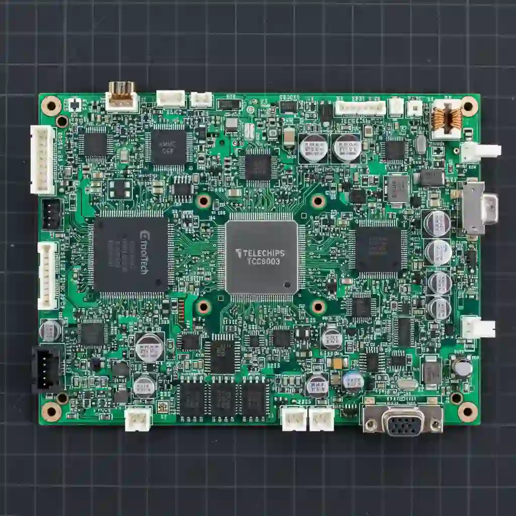
Automotive vision systems and inertial measurement units (IMUs) form the backbone of perception and localization in advanced driver-assistance systems (ADAS) and autonomous vehicles. From a PCB engineering perspective, these sensors impose strict requirements on signal integrity, noise performance, power delivery, thermal management, and hardware-level security. Effective PCB design directly governs the achievable signal-to-noise ratio (SNR), dynamic range, and long-term reliability of image sensors and IMUs while enabling robust sensor fusion for visual SLAM.
SNR in Automotive Image Sensors and PCB Noise Mitigation Strategies
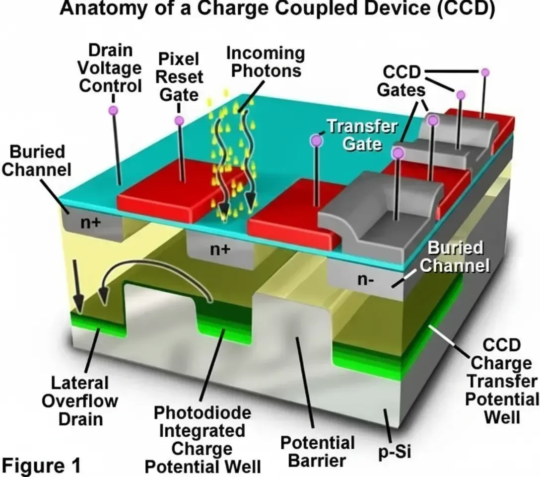
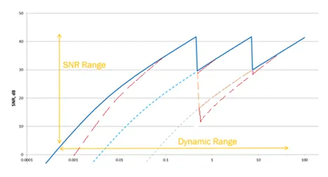
Signal-to-noise ratio determines how clearly an image sensor can distinguish scene details from electronic noise, especially in low-light or high-temperature automotive environments. PCB layout plays a decisive role in preserving SNR.
High-speed serial interfaces (MIPI CSI-2, SLVS-EC) require controlled-impedance differential pairs, minimal via stubs, and continuous reference planes to reduce crosstalk and return-path discontinuities. Dedicated analog and digital power domains, combined with low-ESR decoupling capacitors placed close to sensor pins, suppress switching noise that would otherwise degrade SNR. Ground plane segmentation and shielding cans around sensitive analog sections further isolate image sensor front-ends from high-speed digital processing and power electronics.
Dynamic Range Enhancement Through PCB Power Integrity and ADC Integration
Automotive scenes exhibit extreme contrast—from bright sunlight to deep shadows—demanding high dynamic range (HDR) performance. On the PCB, this translates to clean, low-ripple power rails for the image sensor's analog front-end and precise reference voltages for the analog-to-digital converters (ADCs). Multilayer stack-ups with dedicated power planes and sufficient copper weight minimize voltage drops and inductive noise. Careful placement of bypass capacitors and use of low-dropout regulators (LDOs) or switching regulators with spread-spectrum modulation help maintain the sensor’s full dynamic range. Thermal vias and copper pours around the sensor package also prevent temperature-induced gain and offset drift that would compress dynamic range over the vehicle’s operating temperature range.
Cybersecurity Threats to Automotive Image Sensors and Hardware-Level PCB Protections
Image sensors are increasingly targeted by cyberattacks that attempt to inject false data or extract proprietary information. PCB-level countermeasures include hardware root-of-trust implementations, secure boot circuitry, and encrypted data paths between the sensor and domain controller. Tamper-evident enclosures, mesh shielding layers within the PCB stack-up, and side-channel attack mitigation through balanced power distribution networks strengthen physical security. Automotive PCBs must also support functional safety requirements (ISO 26262) by incorporating redundant traces or watchdogs that detect communication failures or anomalous sensor behavior.
Rectangular Image Geometry and Sensor Packaging on PCBs
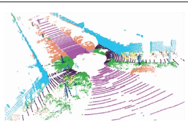
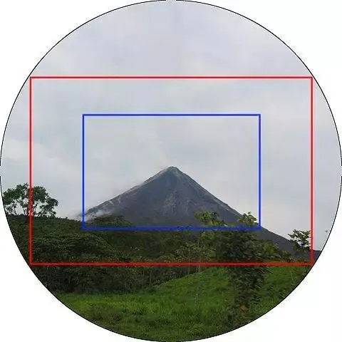
Camera images appear rectangular because image sensors are fabricated with rectangular pixel arrays aligned to the optical axis. On the PCB, this geometry influences mounting orientation, lens alignment tolerances, and thermal expansion matching between the sensor package and board. Precise fiducial placement and controlled warpage of the PCB substrate ensure consistent optical alignment across temperature cycles. HDI technology allows finer pitch routing for high-resolution sensors while maintaining mechanical stability for vibration-intensive automotive environments.
Automotive Memory Architectures for Image Processing and PCB Integration
High-resolution automotive cameras generate massive data streams that require fast, reliable memory for buffering, HDR merging, and temporary storage before transmission to the central processor. LPDDR4/5, DDR4/5, and high-endurance NOR/NAND flash are commonly integrated on the same PCB as the image sensor or vision processor. PCB designers must optimize wide memory buses with length-matched traces, proper termination, and robust power delivery networks to support high data rates without compromising signal integrity. Thermal management of memory packages becomes critical during continuous HDR processing, often requiring thicker copper layers or embedded heat spreaders.
IMU Sensors in Autonomous Vehicles and PCB Performance Optimization
Inertial measurement units provide high-frequency acceleration and angular velocity data essential for visual-inertial odometry and dead-reckoning when GNSS or camera data are unavailable. PCB design directly affects IMU accuracy through vibration isolation, thermal stability, and clean analog signal paths. Placing IMUs away from high-current switching regulators and using dedicated low-noise power rails minimizes interference. Rigid-flex or stiffened PCB sections around the IMU reduce mechanical coupling from vehicle vibration. Temperature compensation algorithms benefit from stable board-level thermal gradients achieved through balanced copper distribution and strategic via placement.
Improving IMU Performance via PCB Layout and Sensor Fusion Techniques
Key PCB techniques for enhancing IMU performance include minimizing trace inductance in the power and ground paths, employing star-grounding topologies, and adding local decoupling networks. For visual SLAM, tight synchronization between camera frames and IMU samples requires low-jitter clock distribution across the board.
High-layer-count PCBs with embedded clock planes and precise length matching support the microsecond-level timing accuracy demanded by tightly coupled sensor fusion algorithms. Automotive qualification further necessitates vibration-resistant via structures and materials with appropriate coefficients of thermal expansion.
Conclusion
Delivering reliable automotive perception and localization ultimately depends on PCB-level engineering decisions that simultaneously optimize SNR, dynamic range, power integrity, thermal performance, hardware security, and sensor synchronization. As image resolutions climb and SLAM algorithms become more computationally intensive, early collaboration between sensor architects and PCB manufacturers is essential to achieve the required signal quality, functional safety, and long-term durability under harsh automotive conditions. By applying rigorous stack-up design, controlled-impedance routing, advanced thermal management, and automotive-qualified fabrication processes, engineering teams can produce vision and IMU subsystems that meet the stringent demands of next-generation ADAS and autonomous driving platforms. Aivon's expertise in high-reliability, automotive-grade PCB manufacturing enables partners to navigate these complex trade-offs with confidence, delivering boards that fully realize the performance potential of modern image sensors and IMUs.