CMOS image sensors (CIS) have become the dominant technology for capturing high-quality images in smartphones, automotive cameras, industrial vision systems, and medical devices. In PCB manufacturing and design, integrating CIS devices requires precise attention to signal integrity, power distribution, thermal management, EMI/EMC control, material selection, and high-density interconnect (HDI) processes. Proper PCB implementation directly determines sensor performance, image quality, reliability, and manufacturing yield.
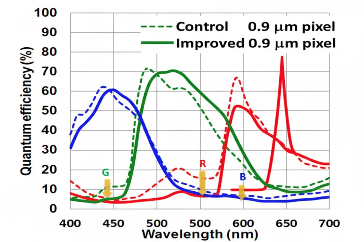
Quantum Efficiency and Spectral Response in PCB Layout
Quantum efficiency (QE) defines how effectively a CIS converts incident photons into electrical charge across the visible and near-infrared spectrum.
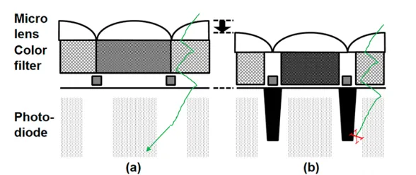
Higher QE improves low-light performance and dynamic range.
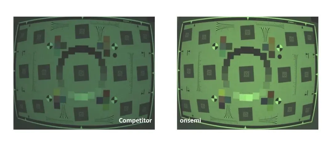
On the PCB, achieving optimal QE involves:
- Precise sensor placement relative to the optical path with minimal obstruction from traces or components.
- Controlled impedance routing for analog pixel outputs and high-speed digital interfaces (MIPI CSI-2 or parallel buses) to preserve signal fidelity.
- Dedicated low-noise power planes and decoupling networks that prevent voltage ripple from degrading sensor performance.
- Use of high-Tg laminates and low-dielectric-loss materials to maintain stable electrical characteristics across temperature variations that could otherwise shift spectral response.
Designers often incorporate optical baffles or shielding layers within the PCB stack-up to reduce stray light and electromagnetic interference that could compromise QE in real-world environments.
Common CMOS Image Sensor Process Defects and PCB Mitigation
Four typical process defects in CMOS image sensors include pixel defects (hot or dead pixels), column defects, row defects, and fixed-pattern noise. While fabrication-level corrections exist, PCB-level strategies significantly improve overall system performance:
- Careful routing of clock and data lines to minimize crosstalk that could exacerbate fixed-pattern noise.
- Symmetric power distribution and star grounding to reduce voltage gradients that contribute to column or row artifacts.
- Thermal vias and copper pours beneath the sensor package to maintain uniform temperature and limit thermally induced defects.
- High-reliability surface finishes (ENIG) and precise pad geometry to ensure stable electrical connections during thermal cycling.
Advanced PCB manufacturing processes such as via-in-pad and micro-via technology enable tighter component spacing while preserving signal integrity around the sensor.
CCD vs CMOS Architecture Trade-offs on PCBs
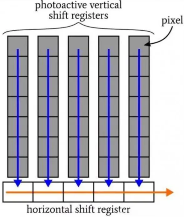
Although CMOS has largely replaced CCD in most applications, understanding architectural differences informs PCB design choices. CCDs require multiple high-voltage clock signals and charge transfer, demanding robust power delivery and low-impedance clock routing on the PCB. CMOS sensors integrate amplification and digitization at the pixel level, allowing simpler power requirements and higher integration density but generating more on-chip digital noise.
PCB implications include:
- Dedicated analog and digital power domains with proper isolation for CMOS designs.
- High-speed differential pairs with controlled impedance for MIPI interfaces common in modern CIS.
- Thermal management solutions that address the higher power density of integrated CMOS readout circuits.
For legacy or specialized high-dynamic-range applications, PCB designers still support CCD modules with appropriate high-voltage isolation and precise timing signal distribution.
Mobile Camera Module PCB Structure and Imaging Principles
Mobile camera modules integrate the CIS, lens assembly, autofocus actuators, and image signal processor (ISP) on compact PCBs.
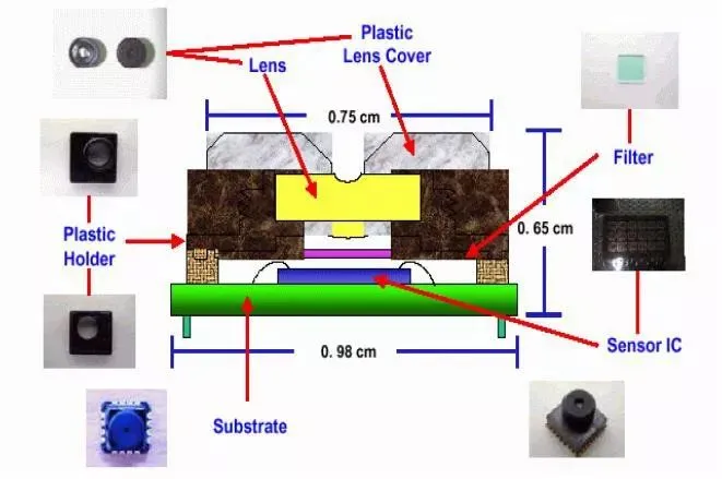
Key design considerations include:
- Rigid-flex or HDI PCBs that accommodate the stacked sensor and lens assembly while maintaining mechanical stability.
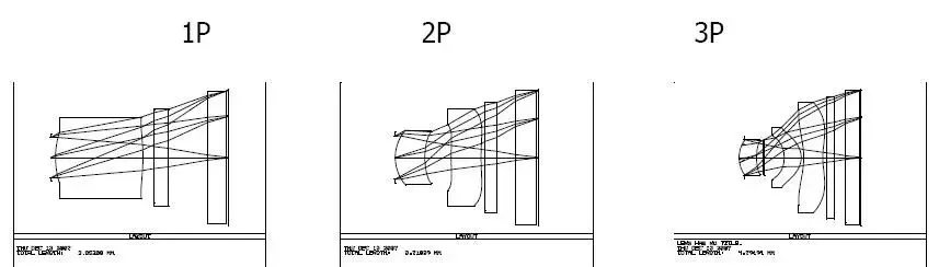
- Precise fiducial placement and tight manufacturing tolerances for optical alignment.
- Miniaturized power management and filtering to support multiple voltage rails required by the sensor, actuator, and ISP.
- EMI shielding and ground plane strategies to prevent interference between the camera module and other smartphone subsystems.
Imaging principles such as rolling shutter versus global shutter further influence PCB timing and synchronization requirements.
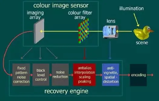
Image Signal Processor Integration and PCB Optimization
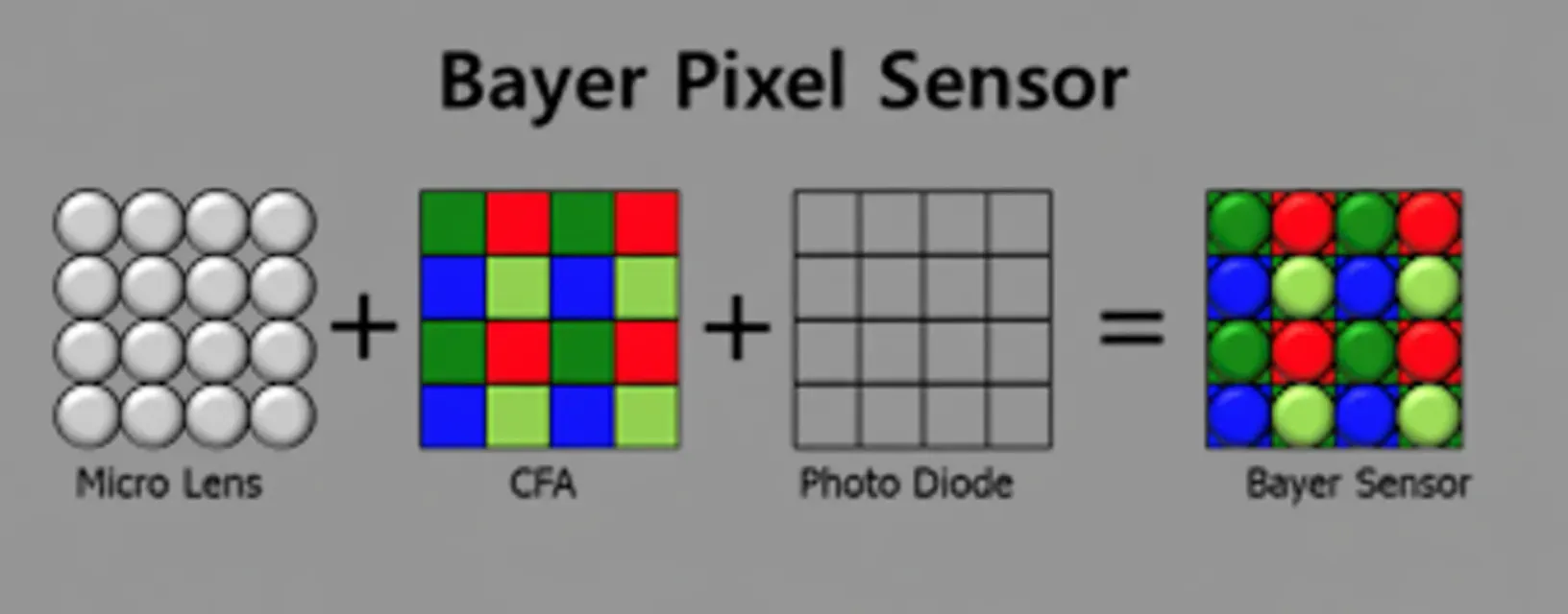
The ISP performs critical functions including demosaicing, noise reduction, white balance, and compression. On the PCB, successful ISP integration demands:
- High-bandwidth memory interfaces and controlled-impedance routing for raw sensor data.
- Efficient thermal paths to dissipate heat from high-performance ISP chips.
- Low-latency interconnects between the CIS and ISP to minimize image artifacts.
- Advanced stack-up designs that support fine-pitch BGA packages and embedded components.
Future trends point toward AI-accelerated ISPs and stacked sensor architectures, increasing demand for HDI, embedded die, and heterogeneous integration on PCBs.
Future Trends and Automotive Safety Applications
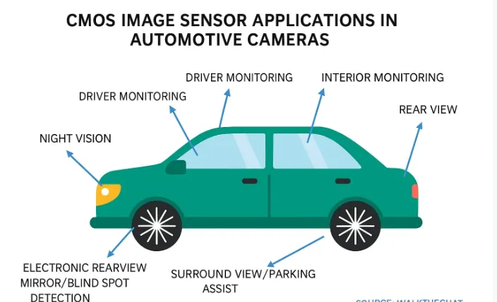
Emerging trends include higher-resolution stacked CIS, event-based sensors, and integration with AI processors. In automotive applications, CIS enable advanced driver-assistance systems (ADAS) and autonomous driving, requiring:
- AEC-Q100 qualified PCBs with enhanced thermal cycling and vibration resistance.
- Redundant power and signal paths for functional safety (ISO 26262).
- Robust EMI shielding and optical window designs that maintain performance under harsh environmental conditions.
PCB manufacturers must support heavy copper, high-reliability laminates, and precise via structures to meet these demanding requirements.
Conclusion
CMOS image sensors deliver exceptional imaging performance only when seamlessly integrated into optimized PCBs. By addressing quantum efficiency, defect mitigation, architectural trade-offs, high-speed signaling, thermal management, and automotive-grade reliability from the earliest design stages, engineers achieve superior image quality, lower noise, and extended product lifespan. As image sensor technology continues to advance toward higher resolutions, AI integration, and automotive safety applications, specialized PCB manufacturing capabilities remain essential. Aivon’s advanced PCB solutions, including HDI, heavy copper, high-Tg materials, and precision RF/analog features, enable the next generation of high-performance imaging systems across consumer, industrial, and automotive markets.