Hall effect sensors detect magnetic fields and convert them into electrical signals, making them essential for current sensing, position detection, speed measurement, and proximity sensing in automotive, industrial, and consumer electronics. In PCB manufacturing and design, successful integration requires careful attention to magnetic field coupling, signal integrity, EMI/EMC mitigation, thermal management, and reliable interconnects. Optimized PCB layout and stack-up directly determine sensor accuracy, noise immunity, and long-term reliability.
Operating Principles and PCB Layout Considerations
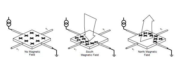
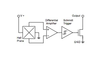
Hall effect sensors operate on the principle that a magnetic field perpendicular to current flow in a conductor generates a measurable voltage (Hall voltage) across the conductor.
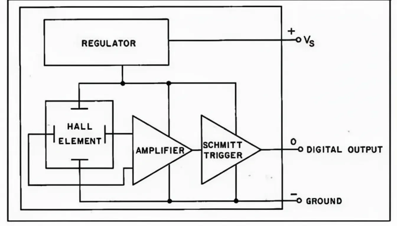
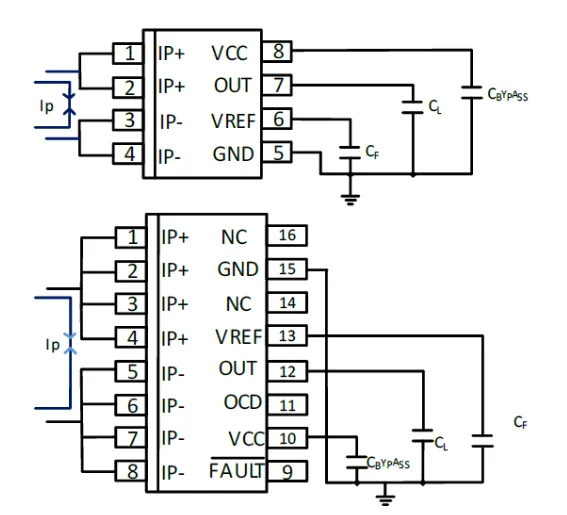
On a PCB, this voltage is typically small and requires immediate amplification or conditioning. Key layout practices include:
- Placing the Hall element close to the magnetic source (permanent magnet or current-carrying conductor) while maintaining consistent orientation.
- Using short, symmetric traces for the Hall voltage output to minimize offset and thermoelectric effects.
- Incorporating dedicated power and ground planes with low-impedance paths to reduce voltage drops and noise.
- Adding decoupling capacitors directly at the sensor power pins to stabilize the bias current.
For current-sensing applications, the PCB trace or bus bar must be routed precisely relative to the sensor to ensure repeatable magnetic field strength, often requiring tight tolerance on copper thickness and trace geometry.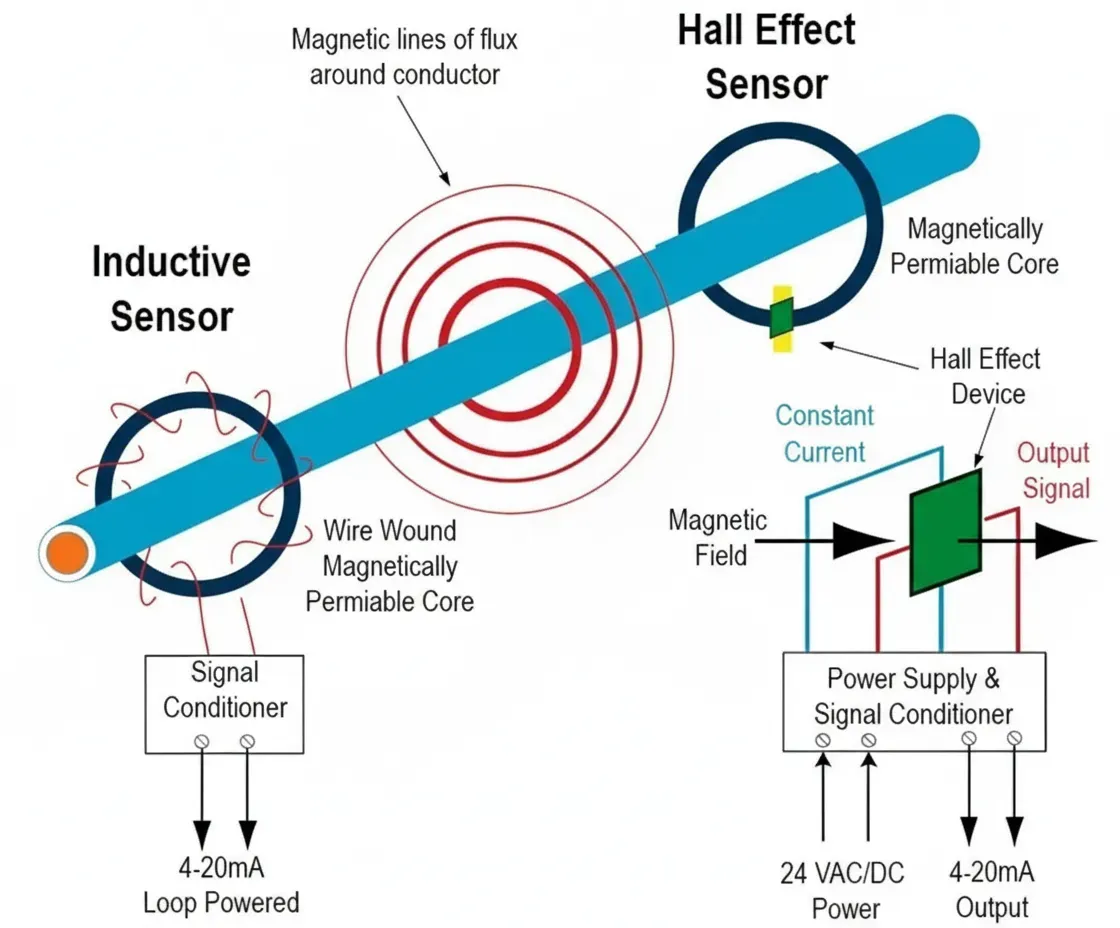
Differential Hall Sensors: Advantages in PCB Design
Differential Hall sensors use two or more sensing elements to measure the difference in magnetic field, rejecting common-mode noise and offsets. This architecture improves accuracy in noisy environments and is particularly valuable for automotive and industrial PCBs. On the board, differential designs benefit from:
- Matched trace lengths and impedances between the two sensing channels.
- Symmetric placement of the sensor package relative to the magnetic field gradient.
- Differential signaling to downstream amplifiers or ADCs, which enhances noise rejection and supports longer trace runs.
- Careful via stitching and ground plane splits to maintain signal integrity across the differential pair.
Compared with single-ended Hall sensors, differential types reduce the impact of PCB warpage, temperature gradients, and external magnetic interference, leading to more stable output over temperature and vibration.
Magnetic Circuit Applications and PCB Integration Strategies
Hall effect sensors are commonly paired with magnetic circuits—permanent magnets, soft magnetic cores, or current conductors—to shape and concentrate the magnetic field.
PCB designers must consider the entire magnetic circuit:
- Magnet placement relative to the sensor and board features (holes, cutouts, or shielding layers).
- Use of ferromagnetic materials or shielding cans on the PCB to direct flux or protect against stray fields.
- Thermal expansion matching between magnets, sensor packages, and the PCB substrate to prevent mechanical stress during temperature cycling.
- Integration of magnetic shielding layers or mu-metal inserts in multilayer stack-ups for high-interference environments.
In motor control and encoder applications, the multilayer PCB often incorporates multiple Hall sensors arranged in precise angular or linear patterns, requiring high-accuracy fiducial placement and tight manufacturing tolerances during fabrication.
Signal Conditioning, EMI Mitigation, and Reliability on PCBs
Hall sensor outputs are susceptible to electromagnetic interference from nearby switching power supplies, motors, or wireless modules. Effective PCB strategies include:
- Guard rings and shielding ground planes around analog signal traces.
- Separation of high-current power paths from sensitive Hall signal lines.
- Use of high-Tg laminates and controlled CTE materials to maintain mechanical stability and sensor calibration over wide temperature ranges.
- Proper via design (multiple parallel vias or filled vias) for thermal dissipation when sensing high currents.
- Conformal coating or potting for environmental protection in harsh conditions.
Reliability considerations encompass solder joint integrity under thermal cycling, drift compensation through calibration at the system level, and selection of automotive-grade or industrial-grade Hall sensors with proven PCB compatibility.
PCB Manufacturing and Material Selection Best Practices
High-performance Hall sensor PCBs often require:
- FR4 or high-Tg materials with low dielectric loss for stable analog performance.
- Heavier copper weights (2–4 oz) for current-sensing traces to handle high amperage without excessive heating.
- Precise drilling and via filling to support dense sensor arrays.
- Controlled impedance routing when differential signals travel long distances.
- Surface finishes such as ENIG for reliable sensor pad connections and long-term corrosion resistance.
Advanced manufacturing processes, including HDI for compact multi-sensor modules and rigid-flex for applications requiring flexible mounting, further enhance integration possibilities.
Conclusion
Hall effect sensors deliver precise magnetic field detection only when seamlessly integrated into well-designed PCBs. By addressing magnetic coupling, differential signaling, EMI control, thermal management, and fabrication constraints from the earliest design stages, engineers achieve higher accuracy, better noise immunity, and extended product reliability. Whether used in automotive powertrains, industrial motor drives, or precision current monitoring, specialized PCB manufacturing capabilities remain essential for realizing the full performance of Hall effect sensors across demanding applications. Aivon’s advanced PCB solutions support the layout precision, material choices, and reliability requirements of modern magnetic sensing systems.