This note summarizes a recent development in hermetic wafer-level sealing for MEMS silicon photonic chips. A research team from KTH Royal Institute of Technology collaborated with EPFL, Tyndall, IMEC, and other institutes to develop a hermetic sealing method for MEMS silicon photonic devices.
Background
Suspended MEMS waveguides often have their SiO2 cladding removed, leaving them sensitive to airflow, dust, and other environmental disturbances. Hermetic sealing is required to mitigate these effects and support commercialization of MEMS silicon photonic devices.
Process Overview
The work used an IMEC iSiPP50G process platform. Local undercut etching was already performed near the waveguides. Additional HF etching was applied to form a vacuum cavity and create suspended waveguides and MEMS structures.
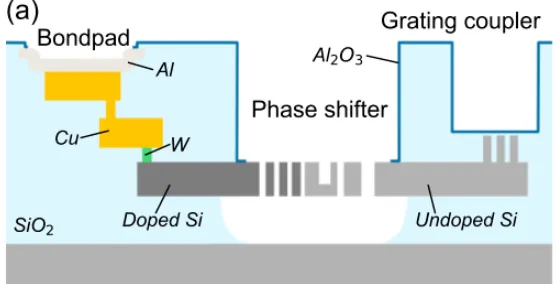
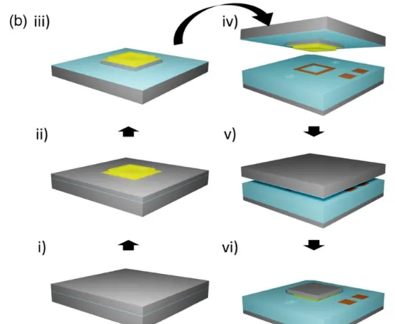
On a separate 100 mm SOI wafer, a 25 μm-thick silicon cap was formed and a 2 μm gold layer was deposited. Matching metal patterns were fabricated on the silicon photonic chip top metal layer. The SOI sealing cap wafer was bonded to the photonic chip using the metal layers as the bonding interface. After removing the handle wafer, a silicon sealing cap covered the MEMS waveguide region that required protection. The overall process flow is shown below.
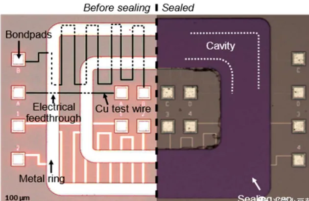
Sealed Chip Structure
A cross-section of the sealed chip is shown below.
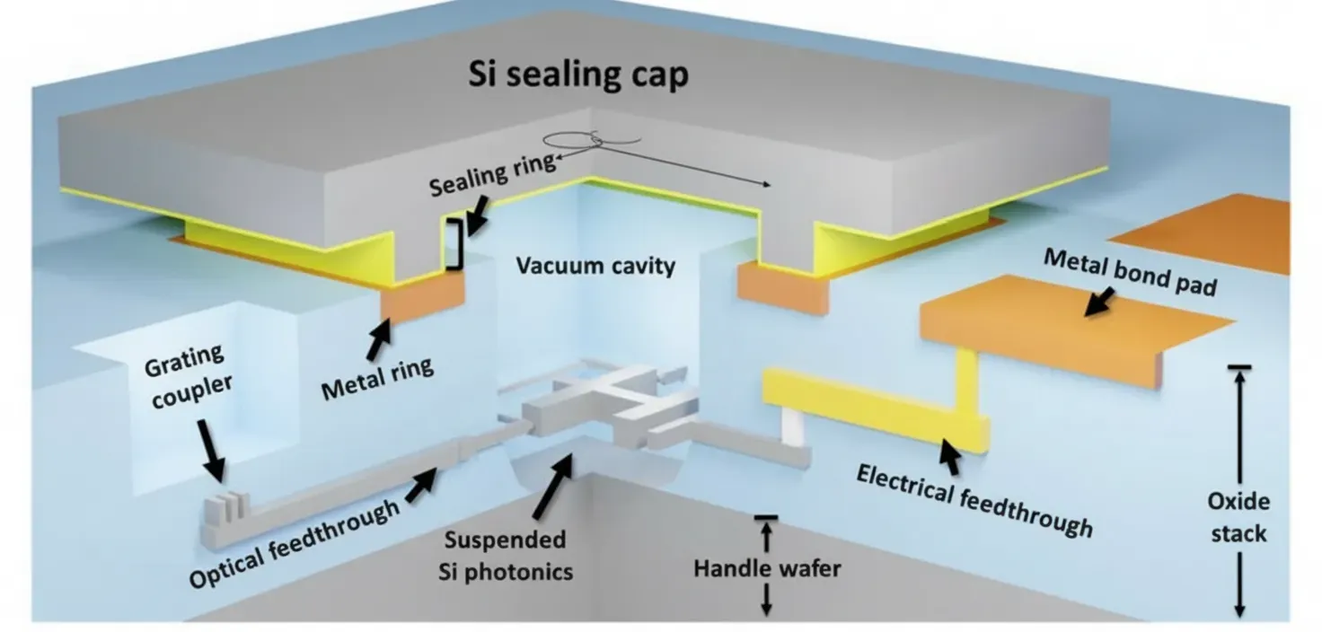
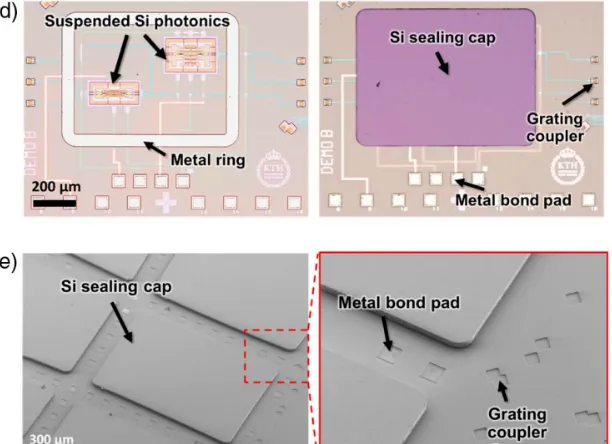
The silicon sealing cap can be dimensioned to cover the MEMS waveguide area as needed. Grating couplers and metal pads were placed outside the sealing cap area to facilitate testing without protection.
Optical and Reliability Characterization
Asymmetric MZIs were characterized before and after sealing. Spectral responses showed no significant changes; peak spectra were close to reference waveguides. Four MZI designs with different lengths and mechanical stability were compared using extinction ratio (ER) spectra. The most fragile cantilever design failed (device B in the figure), while the other three designs retained high ER values.
Sealed phase shifters showed substantially improved phase stability. The 3 dB modulation bandwidth increased from 213 kHz to 776 kHz. Under 36 V DC drive, a pi/2 phase shift was achieved.
Hermeticity Assessment
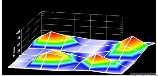
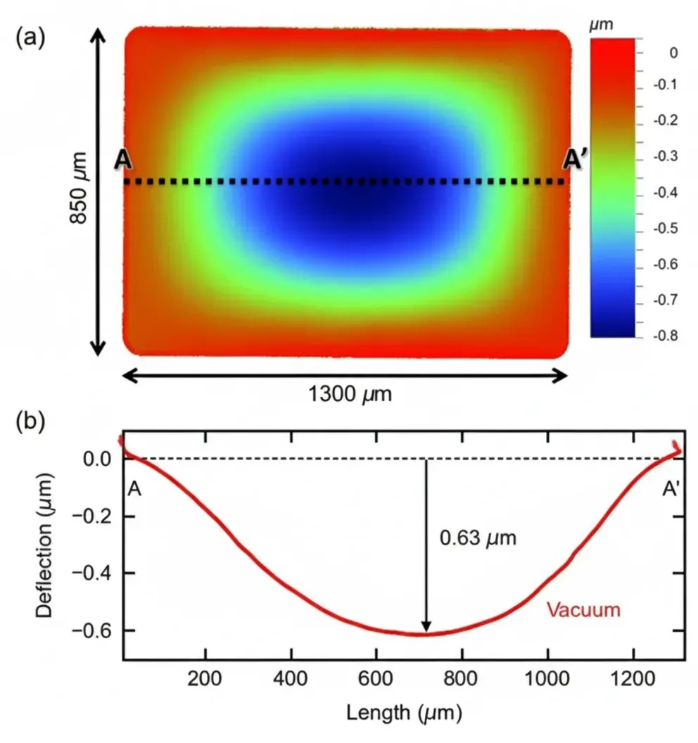
Hermeticity of the sealing cap was evaluated with an optical profilometer to measure cap deflection. The maximum center deflection was 0.63 μm, corresponding to an internal cavity pressure of a few millibar. Results are shown below.
Out of 128 cavities from four dies (two near the wafer center, two near the wafer edge), 115 passed hermeticity testing, yielding nearly 90% yield. After storing the wafer for 21 days, hermeticity remained within specifications. Wafer singulation did not affect hermeticity. These tests support the reliability of the sealing approach.
Design Flexibility and Integration
Sealing cap shapes are flexible and not limited to rectangles; L-shaped, triangular, and donut geometries are possible. The image below shows a donut-shaped cap with metal pads on both sides for electrical testing.
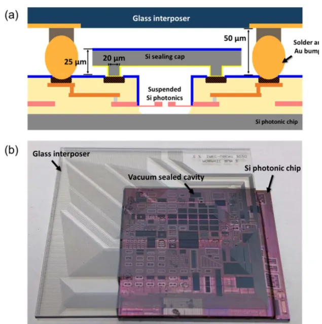
Because the silicon cap is only 25 μm high while typical bumps are around 50 μm, other chips can be flip-chipped onto the sealed MEMS silicon photonic chip. The schematic below illustrates a glass interposer flip-chipped to the silicon photonic chip; the interposer in the example uses 599 bumps.
Summary
The KTH group used metal bonding to form a silicon sealing cap over MEMS waveguides, protecting suspended waveguides from airflow and environmental disturbance. The approach improved device stability and yield while using relatively simple process steps. A series of reliability tests demonstrated the method's robustness. MEMS phase shifters remain attractive for dense photonic integration due to short device length and zero static power, despite modest bandwidths on the order of hundreds of kilohertz.
A previous MEMS-based photonic computing system demonstrated at Hot Chips 2019 raised questions about packaging and system reliability. This wafer-level hermetic sealing technique offers a practical path toward more robust MEMS silicon photonic devices. Next steps likely include validating flip-chip integration of electronic chips onto the hermetically sealed MEMS photonic chips.