What Does Modulation Do? 5G Modulation Methods
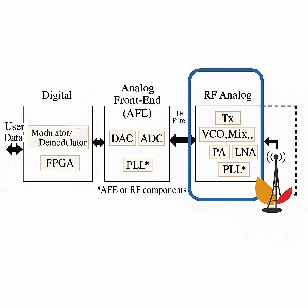
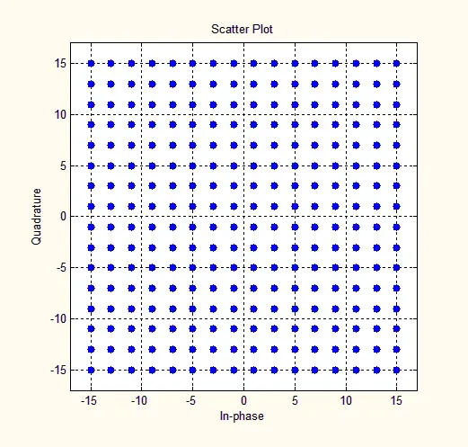
Technical overview of modulation in 5G: PSK and QAM, constellation diagrams, and IQ modulation/demodulation principles for mapping bits to carrier amplitude and phase.
Mobile Communications represents a dynamic field within electronics and PCB design, encompassing the technologies that enable wireless connectivity in devices ranging from smartphones to IoT sensors. This category delves into the foundational principles and advanced innovations driving seamless data transmission, voice calls, and network integration. Whether you are an engineer optimizing circuit boards for high-frequency signals or a developer integrating modules into embedded systems, the content here addresses the core challenges and opportunities in this rapidly evolving domain. Our articles offer comprehensive guides on essential topics such as antenna design, RF module selection, and PCB layout strategies tailored for mobile applications. Tutorials provide step-by-step instructions for implementing protocols like Bluetooth, Wi-Fi, and cellular standards, while insights explore emerging trends including 5G deployment and edge computing. Best practices focus on ensuring signal integrity, power efficiency, and electromagnetic compatibility, helping you avoid common pitfalls in real-world projects. The practical value of Mobile Communications extends to diverse industries, from consumer electronics to automotive and healthcare. By understanding these concepts, professionals can enhance device performance, reduce interference, and comply with regulatory standards. Articles in this category equip readers with actionable knowledge to tackle design complexities, foster innovation, and adapt to technological shifts. As you navigate through the posts, you will gain a deeper appreciation for how mobile technologies underpin modern connectivity, empowering you to apply these principles in your own work.
Technical overview of modulation in 5G: PSK and QAM, constellation diagrams, and IQ modulation/demodulation principles for mapping bits to carrier amplitude and phase.
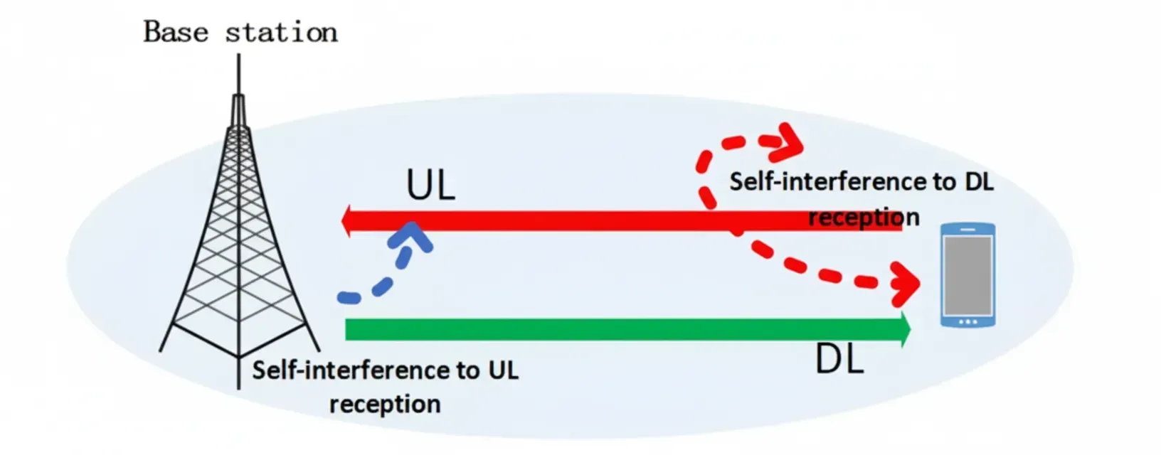
Technical overview of 5G NR architecture, use cases and waveform evolution, including massive MIMO, full?duplex operation and NR operating bands for engineers.
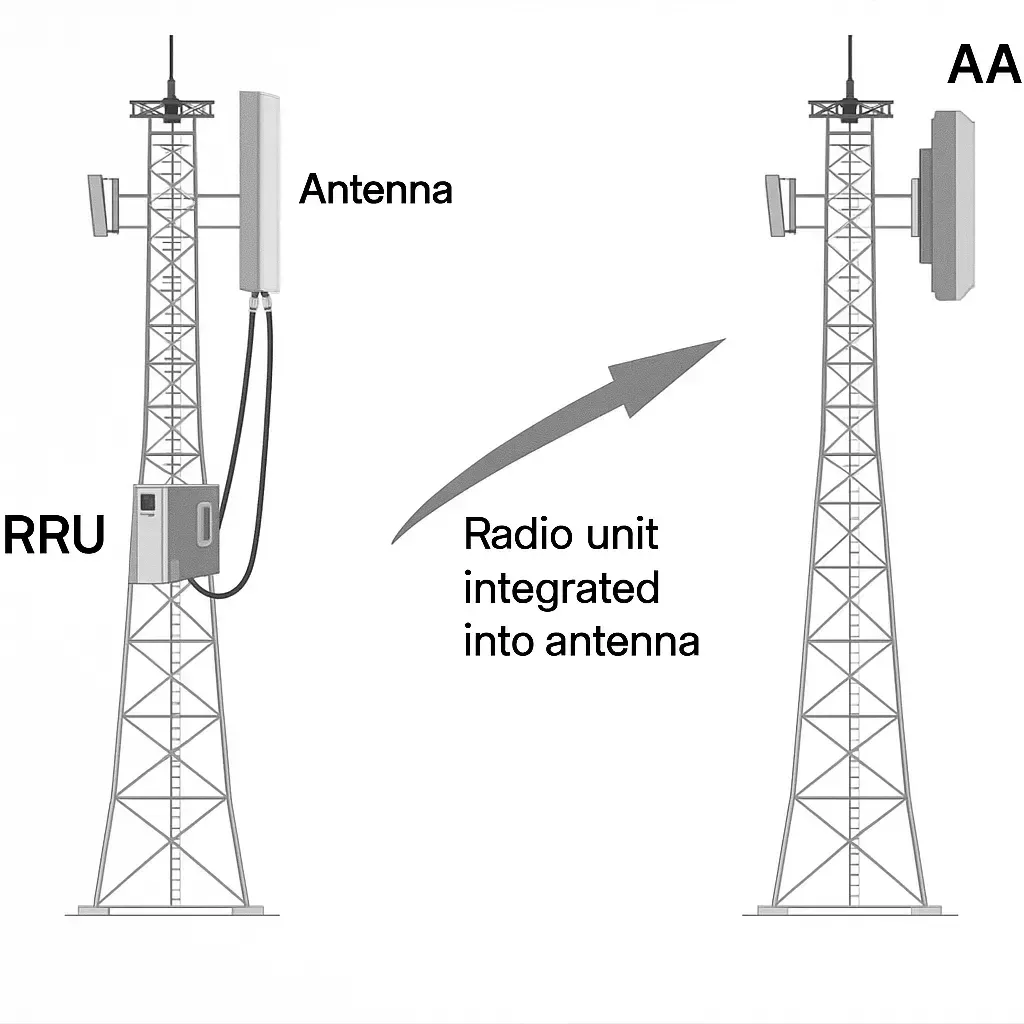
Overview of 4G and 5G base stations: site components, installation steps, and differences introduced by massive MIMO, with deployment procedures for antennas and cabling.
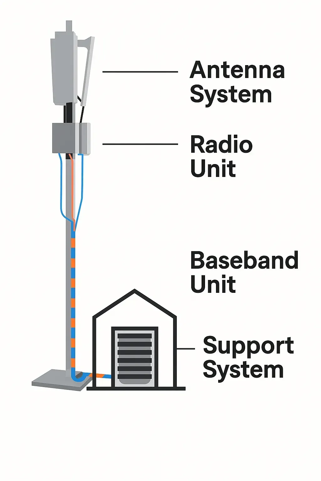
Technical overview of base station components—antenna-feeder system, RRU (radio frequency unit), baseband unit and equipment room—explaining function and RF exposure.
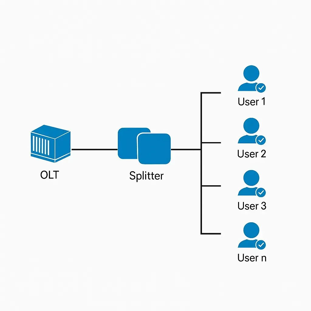
Technical overview of optical access networks detailing OLT and ONU roles, architecture, interfaces, and deployment types (FTTH/FTTB/FTTC) for fiber access.
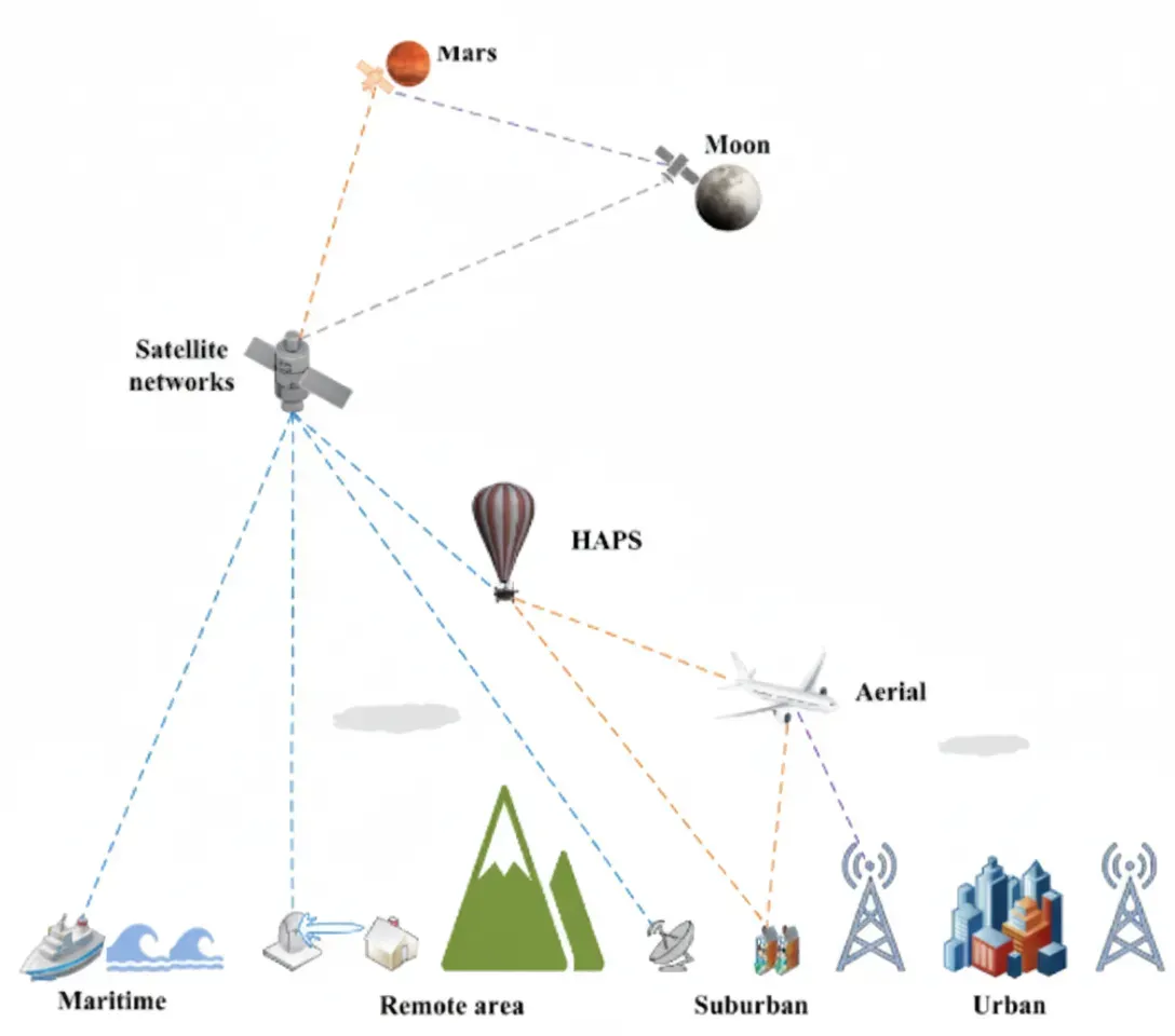
Survey of massive MIMO evolution for 6G: intelligent surfaces (IOS/IRS), cell?free architectures, AI, positioning/sensing, and non?terrestrial network challenges.
Technical Q&A on electromagnetic shielding and skin depth, transmission losses, lens optics and fog, combustion state, atmospheric oxygen effects, and quantum determinism
Explore 5G LAN standards from Release 16 to 18, industrial application requirements, and the critical role of high-frequency PCBs, low-loss materials, and manufacturing processes in enabling reliable 5G LAN infrastructure for smart manufacturing and enterprise networks.
Analysis of SA 5G-to-4G handover failures: MME counters and EMS signaling found MME–eNB coupling and gNB configuration/link issues; RAN corrections restored success.
Technical survey of millimeter-wave semiconductor advances and phased-array beamforming for 5G/6G, covering materials, IC/process design, packaging, testing, and DARPA MIDAS work.
Analysis of faded signal bar and icon loss on iPhone 14: 4G/5G interaction triggered an SDM power?saving code issue causing a modem crash; fixed in Apple update.
Case study: iPhone 13 signal bars flickering caused by repeated PDU session teardown/rebuild after SMS validation error due to incorrect My Number setting.