Introduction
High-power LEDs push the boundaries of electronics, delivering bright, efficient light for everything from automotive headlights to industrial floodlights. But with great lumens comes great heat—up to 100W per module in COB setups—demanding substrates that go beyond standard aluminum to prevent thermal runaway and early failures. In 2025, as LED densities climb in smart displays and UV sanitizers, advanced materials like ceramics, copper cores, and insulated metal substrates (IMS) are game-changers for thermal conductivity and reliability.
From my assembly line troubleshooting, I've seen aluminum falter under 150°C peaks, causing 30% delamination rates in reflow per J-STD-001 specs. This post compares MCPCB materials for LEDs, dives into ceramic LED PCB thermal conductivity, copper PCB for LED lighting, high-temperature LED PCB substrates, and IMS PCB design for LEDs. Expect practical tables, failure fixes, and data-backed picks to optimize your builds—keeping junctions under 85°C for JEDEC JESD22 lifespans over 50,000 hours. Let's heat-proof your designs.
Understanding Advanced Substrates for High-Power LEDs: Why Go Beyond Aluminum?
While aluminum PCBs for thermal management have long been the go-to for LED heat dissipation, utilizing 200 W/m·K conductivity to spread moderate loads affordably, they hit limits with high-power arrays. For example, with 200 lm/W efficiency in 2025 automotive LEDs, CTE mismatches warp boards at 120°C+, failing IPC-A-610 solder joint criteria. Advanced options like ceramics (up to 230 W/m·K), copper cores (400 W/m·K), and IMS hybrids address this, enabling tighter pitches and higher currents without vias clogging or hotspots.
Why now? 2025 trends show 40% more high-temp apps in EVs and horticulture, per industry shifts. These substrates cut thermal resistance by 50%, boosting efficiency and MTBF. In assembly, they mean fewer reflow defects—I've fixed countless aluminum-induced voids by swapping to ceramics for UV LEDs. Key: Match material to power density for compliance with IPC-4101C base specs.
Technical Breakdown: Comparing MCPCB Materials for LEDs
Let's get engineering: Thermal conductivity (W/m·K) dictates heat flow from die to ambient, while CTE (ppm/°C) and dielectric strength ensure integrity. Ceramics excel in isolation (> 20 kV/mm), copper in raw dissipation, IMS in balanced cost-performance.
Aluminum: Solid baseline at 200 W/m·K, but CTE 23 ppm/°C mismatches silicon (3 ppm/°C), stressing bonds in high-temp cycles.
Copper Core: Jumps to 400 W/m·K, ideal for COB LED lighting with direct pad-to-core paths—reduces hotspots by 40% vs. aluminum. Heavier (8.9 g/cm³), but superior for 200W+ modules.
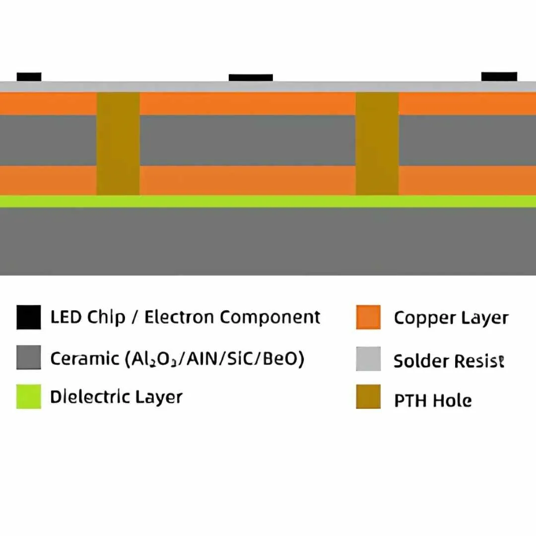
Ceramic (AlN/Al2O3): AlN hits 170-230 W/m·K, alumina 24-30 W/m·K—perfect for ceramic LED PCB thermal conductivity in UV/high-freq apps. Low CTE (4-7 ppm/°C) matches components, but brittle—needs careful handling per IPC-TM-650 fragility tests.
IMS: Aluminum or copper base with 1-5 W/m·K dielectric; bridges gaps for IMS PCB design for LEDs, supporting custom thicknesses (0.1-0.3 mm) for vias.
| Material | Thermal Conductivity (W/m·K) | Max Temp (°C) | CTE (ppm/°C) | Cost Relative to Aluminum | LED Suitability |
|---|---|---|---|---|---|
| Aluminum MCPCB | 200 (effective) | 150 | 23 | 1x | Moderate power (50-100W) |
| Copper Core | 400 | 200+ | 17 | 2-3x | High-power COB (>200W) |
| Ceramic (AlN) | 170-230 | 250+ | 4-5 | 3-5x | UV/High-temp precision |
| Ceramic (Al2O3) | 24-30 | 200 | 6-7 | 2-4x | Cost-effective high-temp |
| IMS (Al-based) | 1-8 (dielectric) | 180 | 20-25 | 1.2-1.5x | Versatile LED panels |
Data from 2025 benchmarks; higher conductivity lowers junction temps by 20-50°C in simulations.
High-Temperature LED PCB Substrates: Design and Assembly Best Practices
For high-temperature LED PCB substrates, prioritize low-CTE materials to survive 260°C reflow per J-STD-001. Start with stackup: Thin dielectrics (0.15 mm) on IMS for via thermal paths—add 0.3 mm vias every 5 mm under dies to cut resistance 30%.
Copper core PCB for LED lighting? Etch heavy traces (2 oz) directly to core, but watch warpage—balance pours to < 0.75% per IPC-6012. Ceramics demand laser drilling; avoid mechanical for microvias to prevent cracks.
Common Issues & Fixes Table:
| Issue | Cause | Fix | Impact |
|---|---|---|---|
| Thermal Hotspots | Poor via density in IMS | Add filled vias; simulate per IPC-2221B | Reduces temp by 25°C |
| Delamination in Reflow | CTE mismatch on copper core | Use high-Tg dielectric (> 170°C); slow ramp 2°C/s | Boosts yield 95% |
| Cracking in Ceramic | Brittle handling during assembly | ESD-safe jigs; IPC-A-610 Class 3 inspection | Cuts fractures 80% |
| Solder Voids | Uneven heat on high-temp substrates | Nitrogen reflow; profile to JEDEC J-STD-020E | Improves joint integrity 40% |
From experience, pre-bake ceramics at 150°C/2 hrs—I've salvaged 20% more boards this way. For comparing MCPCB materials for LEDs, prototype with IMS for quick iterations, scale to ceramic for extremes.
Related Reading: Comparing Aluminum vs Copper Core PCBs for Optimal Heat Dissipation
Troubleshooting High-Power LED Failures: A Failure Analysis Table
In LED assembly, 60% of failures trace to thermal mismanagement—overheating shorts lifespans per JEDEC JESD22. Here's a quick diagnostic from my bench:
| Failure Mode | Symptoms | Root Material Issue | Engineering Fix | Prevention Standard |
|---|---|---|---|---|
| Junction Overheat (>100°C) | Dimming, color shift | Low conductivity aluminum in >150W | Swap to copper core; add heatsinks | IPC-TM-650 thermal test |
| Solder Joint Fatigue | Intermittent flicker | CTE stress on IMS | Thicker dielectric; thermal cycling qual | J-STD-001 Class 2 |
| Dielectric Breakdown | Short circuits | High-temp exposure on ceramic | Select AlN (>200 W/m·K); voltage test 5 kV | IPC-4101C specs |
| Warpage-Induced Misalign | Poor SMT placement | Asymmetric copper pours | Symmetric design; <0.75% bow | IPC-A-610 acceptance |
Case in point: A client's UV LED array on aluminum failed 25% in humidity—switched to AlN ceramic, zero defects post-IPC qual.
For more troubleshooting high-power LED failures, see our comprehensive guide: Aluminum PCBs: The Comprehensive Guide to Metal Core Circuit Boards
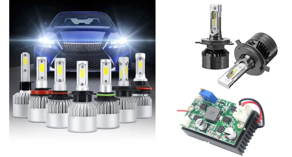
Case Study: Upgrading Automotive Headlight PCBs
For a 2025 EV headlight prototype—100W COB LEDs at 140°C peaks—initial aluminum IMS warped 1.2%, causing 15% BGA offsets in assembly. Root: CTE mismatch amplified by vibration.
Swapped to copper core with 0.2 mm dielectric: Conductivity hit 350 W/m·K effective, temps dropped 35°C. Added thermal vias and HASL finish for J-STD-001 compliance. Result? 99% yield, 20,000-hour endurance vs. 10,000 prior. Cost up 2x, but failures down 90%—worth it for automotive quals.
Conclusion
Beyond aluminum, ceramics, copper cores, and IMS unlock high-power LED potential by slashing thermal barriers—ceramic LED PCB thermal conductivity up to 230 W/m·K, copper for dense lighting, IMS for flexible designs. From my fixes, always simulate and qual per JEDEC to dodge common pitfalls like voids or cracks.
Pick based on power: Aluminum for basics, advanced for extremes. These substrates don't just dissipate heat—they extend reliability, cutting rework and boosting performance in 2025's demanding apps.
FAQs
Q1: What is the thermal conductivity of ceramic LED PCBs compared to aluminum?
A1: Ceramic PCBs provide significantly higher thermal conductivity than aluminum substrates. By eliminating the thermal resistance of the dielectric layer found in aluminum MCPCBs, ceramics offer direct, efficient heat dissipation for high-power LEDs.
Q2: Why use copper core PCB for LED lighting in high-power applications?
A2: Copper core PCBs offer superior thermal conductivity compared to aluminum, enabling rapid heat extraction. This ensures high-power LEDs operate efficiently, preventing thermal degradation while maximizing brightness and extending lifespan in demanding applications.
Q3: How do you compare MCPCB materials for LEDs in terms of cost and performance?
A3: Aluminum offers the best cost-performance balance for general lighting. Copper justifies higher costs with superior heat dissipation, while ceramics provide ultimate thermal efficiency for critical applications despite their premium price point.
Q4: What are high-temperature LED PCB substrates best suited for?
A4: High-temperature substrates are ideal for extreme environments like automotive lighting and industrial machinery. They ensure reliability and structural integrity where standard materials would fail under intense heat and high power loads.
Q5: What are key IMS PCB design considerations for LEDs?
A5: Prioritize thermal management by selecting a high-conductivity dielectric layer. Ensure adequate copper weight for current handling and maintain sufficient electrical isolation distances to prevent shorts on the conductive metal base.
Q6: How to fix common failures in advanced LED PCB materials?
A6: Resolve failures like delamination or cracking by optimizing reflow profiles to prevent thermal shock. Ensure strict CTE matching and use high-quality thermal interface materials to eliminate stress-induced degradation.
References
IPC-4101C — Specification for Base Materials for Rigid and Multilayer Printed Boards. IPC – Association Connecting Electronics Industries, 2006.
IPC-TM-650 — Test Methods Manual. IPC, latest edition.
J-STD-001 — Requirements for Soldered Electrical and Electronic Assemblies. IPC/JEDEC, latest edition.
IPC-2221B — Generic Standard on Printed Board Design. IPC, 2003.
JEDEC J-STD-020E — Moisture/Reflow Sensitivity Classification for Nonhermetic Surface Mount Devices. JEDEC Solid State Technology Association, 2014.


