Why Create a Printed Circuit Board for a Weather Station?
Designing a dedicated PCB is fundamental for any system collecting and processing environmental data such as temperature, humidity, pressure, or wind speed. This approach offers unparalleled control, allowing you to tailor component selection precisely to your project's demands—whether for a personal setup, educational endeavor, or a more advanced professional application. Online design tools make this accessible, enabling the creation of compact and efficient boards without the need for expensive software or extensive prior experience.
Using freely available PCB software provides significant cost savings while still granting access to powerful features. These often include robust schematic design, circuit simulation capabilities, and comprehensive layout tools. Furthermore, many online platforms seamlessly integrate with manufacturing services, simplifying the transition from a digital design to a tangible product. This guide will explore how to achieve this using a user-friendly browser-based design tool.
Getting Started with Browser-Based PCB Design Software
Before you delve into the actual design process, the first step involves establishing your workspace within a complimentary online PCB design platform. These tools operate directly within your web browser, eliminating the need for any downloads or installations. They typically come equipped with extensive component libraries, intuitive schematic editors, and versatile layout tools, all available without charge.
Begin by registering an account on your chosen browser-based design platform. Once logged in, take a moment to acquaint yourself with the user interface. Most platforms feature a central dashboard where new projects can be initiated. Select the option to create a new schematic, as this marks the initial phase in developing your weather station PCB. It’s also crucial to ensure you have a stable internet connection, as the software functions exclusively online.
Planning Your Weather Station's Electronic Circuit
What Components Do You Need?
Before embarking on the design phase, it's essential to meticulously define the components and intended functionality of your weather station. A standard weather station circuit typically incorporates several key elements:
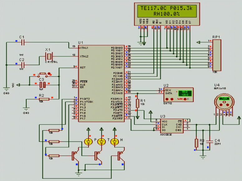
● Microcontroller: This serves as the brain, processing data from sensors. Options like an ESP32 are popular due to integrated Wi-Fi connectivity for data transmission.
● Environmental Sensors:
○ Temperature and Humidity: A sensor such as the DHT22 is a common choice.
○ Atmospheric Pressure: A BMP280 sensor can measure barometric pressure.
● Power Management: A voltage regulator is vital to supply stable power, often 3.3V or 5V, depending on the specific requirements of your chosen components.
● Connectors: These facilitate connections to external modules, antennas, or provide pathways for data transmission.
Considering Power and Communication Protocols
Beyond component selection, careful consideration of power requirements and communication protocols is paramount. For example, if your microcontroller operates at 3.3V but a specific sensor demands 5V, you'll need to integrate voltage level shifters or design for a dual power supply. Similarly, plan how your weather station will transmit data—whether via Wi-Fi, Bluetooth, or a wired connection—as these decisions will significantly influence both your schematic and the final PCB layout.
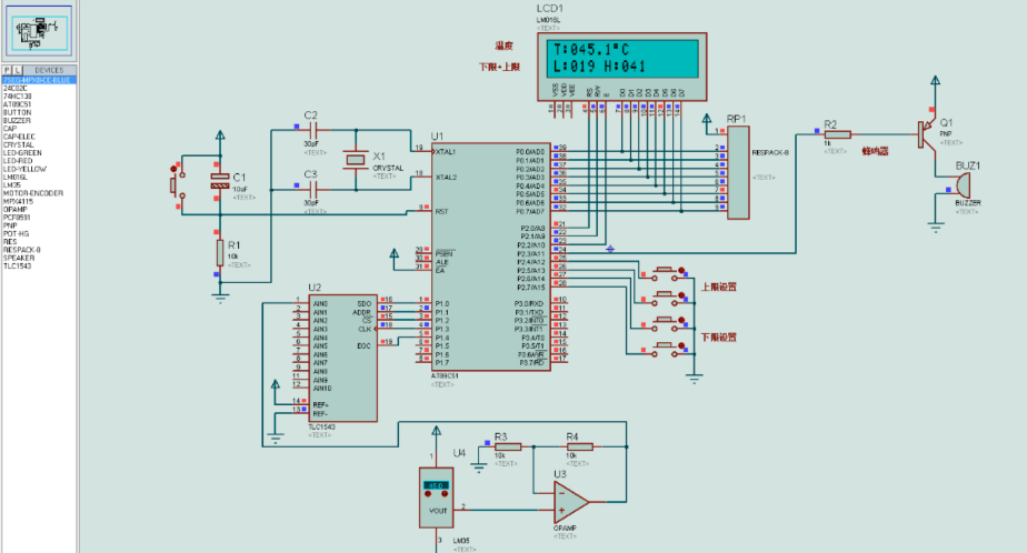
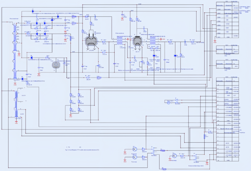
How Do You Create the Schematic for a Weather Station?
With your circuit plan established, the next stage involves constructing the schematic, which acts as a detailed electrical blueprint of your circuit. Within your online design tool, open the schematic editor and begin by adding the planned components from the provided library. Search for specific parts like your chosen microcontroller and sensors. If a particular component isn't readily available, most platforms offer capabilities to create custom symbols or import existing ones.
Position the components logically onto the schematic canvas and establish connections between them using virtual wires. For instance, link the data output pin of a temperature sensor to an appropriate digital input pin on your microcontroller. Ensure all power connections are correctly made, incorporating necessary resistors or capacitors for circuit stability. A common engineering practice is to place a small (e.g., 0.1µF) decoupling capacitor close to the power pins of integrated circuits; this helps filter out electrical noise.
For enhanced clarity, label your connections, also known as "nets," especially for power lines (VCC, GND) and critical data paths. Always cross-reference pin assignments with component datasheets to prevent errors. Incorrectly connecting a sensor's data pin to the wrong microcontroller pin, for example, could lead to communication failures.
Testing Your Circuit: The Role of Simulation
Many contemporary online PCB design tools incorporate simulation features, allowing you to virtually test your circuit before committing to the physical layout phase. Circuit simulation is invaluable for identifying potential issues such as incorrect connections, voltage discrepancies, or signal integrity problems early on. It's advisable to run a basic simulation to confirm that signals are flowing as expected between all components. For example, verify that your microcontroller can consistently read data from the temperature sensor at the intended frequency, perhaps once per second for periodic environmental readings.
Should the simulation reveal any errors, return to your schematic to correct wiring mistakes or adjust component values. This proactive step can save significant time and prevent costly manufacturing defects down the line.
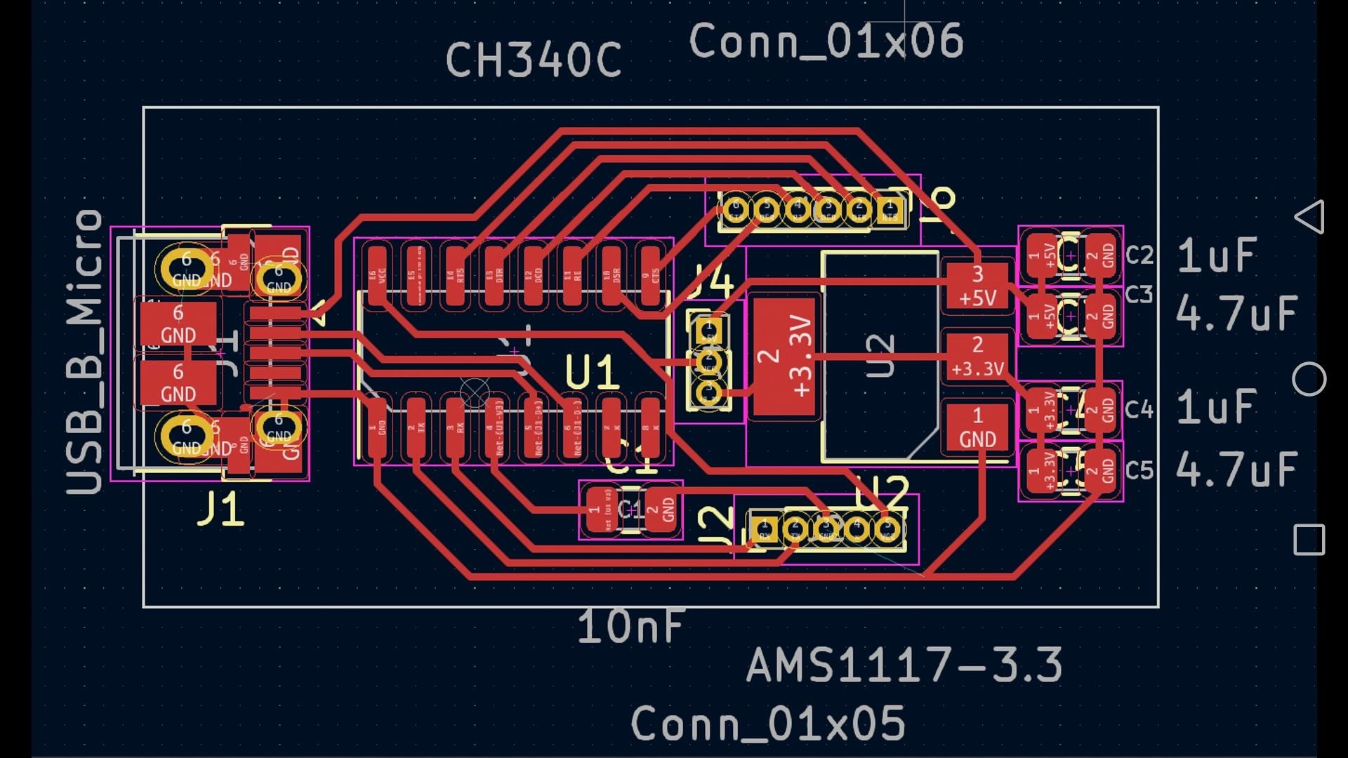
What Are the Steps for Designing the PCB Layout?
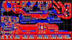
Once your schematic is finalized and has passed simulation checks, the next critical phase is designing the physical PCB layout. Transition to the layout editor within your online tool. Most platforms will automatically transfer all components from your schematic into the layout area, where you can then arrange them on a virtual representation of your circuit board.
Strategic Component Placement
Thoughtful component placement is crucial for optimizing board performance and minimizing potential interference. Arrange components logically to reduce the length of signal traces. For a weather station HDI PCB, it’s beneficial to group related parts together—for example, position the microcontroller close to its associated sensors to minimize signal delays. Power-related components, such as voltage regulators, are often best placed near the edge of the board for easier access to the power input.
Routing Electrical Traces
With components positioned, proceed to route the electrical traces that connect them, guided by your schematic. Employing a solid ground plane is highly recommended to mitigate noise, especially for sensitive analog sensors that are susceptible to interference. Select appropriate trace widths to handle the anticipated current; a 10-mil trace is typically sufficient for low-current signal lines, while power traces might require 20-30 mils or more, depending on the load. Online trace width calculators can provide precise recommendations.
For any high-speed signals (though less common in basic weather stations), keep traces as short and direct as possible to preserve signal integrity. If your weather station uses I2C communication between the microcontroller and sensors, ensure the clock and data lines are routed with similar lengths to prevent timing mismatches.
Performing a Design Rules Check (DRC)
Before concluding the layout, execute a Design Rules Check (DRC) to confirm that your design adheres to standard manufacturing specifications. This automated tool will identify issues like overlapping traces, insufficient clearances between components or traces, and other common errors. Typical clearance values, often between 6-8 mils, are critical for standard quick turn PCB fabrication processes.
Finalizing and Exporting Your PCB Design Files
After meticulously completing the layout, perform a thorough final review for any missed connections, spacing violations, or other discrepancies. Zoom in to closely inspect trace routing and component alignment. Once you are fully satisfied with the design, proceed to export the necessary production files. These are typically generated in Gerber format, which is the industry standard used by manufacturers to fabricate the physical PCB. Most online tools will feature a "Generate Gerber" or similar option within their file menu.
In addition to the Gerber files, it's crucial to export a Bill of Materials (BOM). This document lists every component used in your design, detailing its specifications and required quantities. The BOM is indispensable for the assembly phase and ensures you procure the correct parts. Some advanced online platforms even offer direct integration with PCB manufacturing services, thereby streamlining the entire process from design concept to final production.
Testing and Refining Your Weather Station PCB
Initial Testing and Firmware Upload
Once your PCB has been manufactured and assembled, a comprehensive testing phase is essential. Begin by applying power to the board and use a multimeter to verify voltages at critical points—for example, confirming that the microcontroller is receiving its expected 3.3V or 5V. Next, upload the necessary firmware to your microcontroller. Subsequently, verify that the sensors are providing accurate readings. This can involve comparing the temperature sensor's output against a known ambient temperature to confirm its calibration and functionality.
Iteration: A Key Design Principle
Should any issues surface during testing—such as unexpected noise in sensor readings or communication failures between components—meticulously document these problems. This information is vital for revising your design. Remedial actions might include adjusting trace routing, incorporating additional filtering capacitors, or repositioning certain components. It’s important to remember that iteration is a standard and expected part of the design process, particularly for sophisticated projects like custom weather stations.
Optimizing Your Weather Station PCB for Performance
To enhance the reliability and efficiency of your weather station PCB, consider implementing these design best practices:
● Compactness: Strive to minimize the board's physical dimensions to reduce manufacturing costs. However, always ensure adequate spacing for heat dissipation, especially for components like voltage regulators that can generate significant heat.
● Environmental Resilience: Given that weather stations are frequently exposed to outdoor elements, applying a conformal coating after assembly is highly recommended. This protective layer shields the board from moisture, dust, and other environmental contaminants.
● Power Conservation: Integrate low-power components into your design and consider implementing sleep modes within your microcontroller's firmware to significantly extend battery life, if your station is battery-powered.
● Modularity: Design the PCB with appropriate connectors that facilitate easy replacement or future upgrades of sensors and other modules, enhancing the longevity and adaptability of your system.
Navigating Common Design Obstacles
Designing a weather station PCB can present certain difficulties, particularly for those new to the process. Here are some prevalent challenges and effective strategies for overcoming them:
● Signal Interference: Sensors can be susceptible to electrical noise. Implementing a robust ground plane and ensuring analog signal traces are kept distinctly separate from digital lines can significantly reduce interference.
● Component Acquisition: Certain electronic parts might be difficult to source or have long lead times. Always check the availability of components before finalizing your design, and it’s prudent to identify backup options for critical parts.
● Thermal Management: Components like microcontrollers can generate heat, potentially leading to overheating. Where necessary, integrate thermal vias or small heat sinks, and avoid densely packing heat-generating components.
Conclusion: Empowering Your Weather Station Project
Designing a bespoke PCB for a weather station using accessible online software is an achievable and immensely satisfying endeavor. Through this comprehensive guide, you have acquired the foundational knowledge to systematically plan your circuit, construct an accurate schematic, simulate its functionality, craft a physical layout, and prepare the necessary files for manufacturing. With each step completed, you draw closer to realizing a custom device capable of precisely monitoring environmental conditions tailored to your unique requirements.
The inherent advantages of browser-based PCB design tools lie in their intuitive simplicity and cost-effectiveness. They democratize access to powerful design capabilities, empowering both hobbyists and seasoned professionals to innovate and experiment without substantial financial outlay. Armed with the insights from this guide, embark on your design journey, and witness your weather station project materialize into a functional reality. With persistent effort and practical application, you will undoubtedly master the intricacies of PCB design, opening doors to a multitude of future electronics projects.