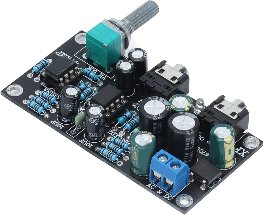
Why Is a Low-Noise Design Crucial for Audio Amplifiers?
In audio amplifier circuits, the presence of noise and interference can significantly diminish sound quality, manifesting as undesirable hums, hisses, or distortion. These issues commonly arise from inadequate grounding practices or suboptimal PCB layouts. Whether the project involves professional audio equipment or a personal DIY endeavor, a low-noise design ensures that the amplified signal remains pristine and faithfully represents the original input. To begin, let’s explore the fundamental principles and methodologies required to achieve this, starting with the bedrock of any truly noise-free design: proper grounding.
Understanding Grounding Practices in Audio Amplifier PCBs
Grounding forms the essential framework of a low-noise audio amplifier PCB. It establishes a universal reference point for all voltages within the circuit and provides a designated path for unwanted currents to return to their source without adversely affecting the audio signal. However, improper grounding can frequently lead to ground loops, electromagnetic interference (EMI), and various other noise-related challenges. Here’s a detailed approach to implementing effective audio amplifier PCB grounding.
The Critical Role of Ground Planes
A robust ground plane, characterized as a large expanse of copper on the PCB, interconnects all ground points within the circuit. This design element effectively lowers impedance and furnishes a low-resistance path for return currents, thereby minimizing noise. For audio amplifiers, a continuous and unbroken ground plane on one dedicated PCB layer can dramatically curtail interference. It is imperative to ensure this ground plane remains as continuous as possible, actively avoiding any splits or cuts that could disrupt the vital return current paths.
Preventing Ground Loops Through Intelligent Design
Ground loops represent a prevalent source of noise in audio systems, often manifesting as a low-frequency hum (typically 50 or 60 Hz, depending on the local power grid frequency). These loops occur when multiple ground paths are established, permitting currents to flow in unintended circular routes, which subsequently induces noise into the sensitive audio signal. Effective ground loop prevention begins with consolidating all ground connections to a single, central point, rather than allowing them to branch into multiple, interconnected paths.
To proactively prevent ground loops, refrain from connecting ground points in a "daisy-chain" sequence. Instead, direct all ground connections to a single, central node, which is frequently situated near the power supply input. This method significantly reduces the potential for currents to circulate through various paths and generate interference. Additionally, it is crucial to maintain a clear separation between high-current paths (such as main power supply lines) and sensitive audio signal grounds to prevent any undesirable noise coupling into the audio circuit.
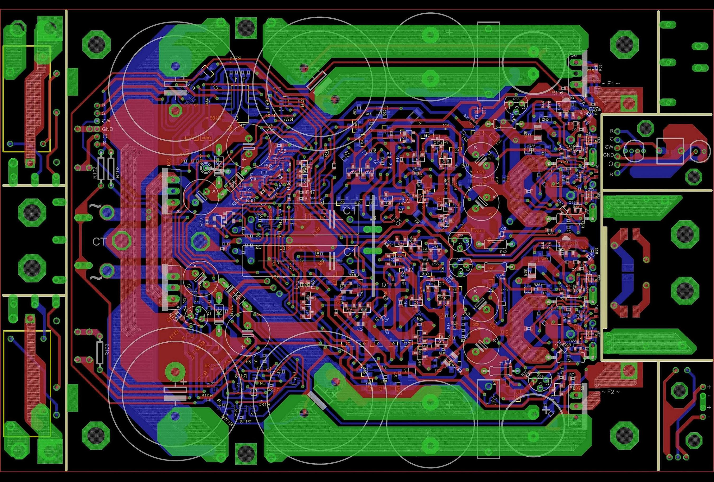
Implementing Star Grounding for Enhanced Noise Reduction
One of the most efficacious noise reduction techniques for audio amplifier PCBs is known as star grounding. In this methodology, all ground connections—whether originating from the power supply, input stage, output stage, or any other components—converge at a singular, central point, often referred to as the "star point." This technique precisely eliminates multiple ground paths, thereby drastically reducing the risk of ground loops and ensuring that return currents do not interfere with delicate audio signals.
To successfully implement star grounding, first identify the primary central ground point, typically located near the power supply or the main filter capacitor. Subsequently, route distinct ground traces from each individual circuit section (e.g., the preamplifier, power amplifier, and input/output connectors) directly to this designated star point. Crucially, avoid sharing ground traces between different circuit sections before they converge at the star point. For multi-layer PCBs, it is best practice to dedicate an entire layer to the ground plane and connect all ground traces to it via dedicated vias at the precise star point location.
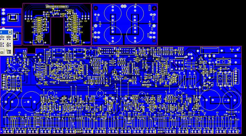
Optimizing PCB Layout for Minimal Noise
A meticulously planned PCB layout for low noise is just as vital as proper grounding. The strategic placement of components, the careful routing of traces, and the clear segregation of analog and digital sections all play critical roles in minimizing unwanted interference. Here are some actionable tips to refine your PCB layout specifically for audio amplifiers.
Thoughtful Component Placement and Segregation
Position sensitive components, such as input stage transistors or operational amplifiers, at a distance from areas prone to high current or significant noise, like power transformers or switching regulators. Group all analog components (e.g., audio inputs and preamplifier circuits) together and ensure their clear separation from any digital components (if present) to prevent crosstalk. For example, keep digital control circuits or microcontrollers on a distinct section of the PCB, ideally with their own dedicated ground plane connected to the main ground at the star point.
Furthermore, orient components to minimize the length of traces for critical signal paths. Shorter traces inherently reduce the likelihood of picking up electromagnetic interference (EMI) and lower overall impedance, thereby helping to preserve signal integrity. For instance, place input capacitors and resistors in close proximity to the amplifier IC or transistor to maintain a concise and tight signal path.
Strategic Trace Routing and Separation
Route audio signal traces with deliberate distance from power supply lines and any high-current paths. If these traces must cross, ensure they do so at a near 90-degree angle to minimize capacitive coupling. Employ wider traces for all power and ground connections to effectively reduce resistance and inductance; aim for a trace width that can comfortably support at least 1.5 times the anticipated current to account for potential heat dissipation and minor voltage drops. As a general guideline, a 10-mil trace on a 1 oz copper PCB can safely handle approximately 0.5 A.
For differential audio signals, route the positive and negative traces in close proximity to each other. This pairing allows for effective cancellation of external noise through common-mode rejection. Keep loop areas exceptionally small by running return paths directly beneath their corresponding signal traces on a different layer, if possible, to minimize susceptibility to magnetic field pickup.
Advanced Noise Reduction Techniques for Audio Amplifier PCBs
Beyond the fundamentals of grounding and layout, several additional noise reduction techniques can significantly enhance the performance of your audio amplifier PCB. These methods specifically target various sources of interference, contributing to a cleaner, more pristine audio signal.
Decoupling Capacitors for Suppressing Power Supply Noise
Noise originating from the power supply can readily couple into the audio signal, particularly in high-gain circuits. To counter this, strategically place decoupling capacitors (typically a combination of 0.1 μF ceramic capacitors and 10 μF electrolytic capacitors) in close proximity to the power pins of every active component, such as operational amplifiers or power transistors. These capacitors effectively filter out high-frequency noise and stabilize the localized voltage supply. For maximum effectiveness, position them within 0.1 inches (2.54 mm) of the power pin, as longer traces introduce greater inductance and consequently diminish filtering efficiency.
Effective Shielding and EMI Protection
External electromagnetic interference (EMI) can severely degrade audio quality, especially in environments rich in strong radio frequency (RF) signals. Employ effective shielding techniques to protect sensitive areas of your PCB. For example, enclosing the input stage or the entire amplifier circuit within a grounded metal enclosure can effectively block external EMI. On the PCB itself, surrounding critical signal traces with an array of ground vias or a solid ground pour can create a localized Faraday cage effect, thereby reducing RF pickup.
If your design incorporates connectors for external inputs or outputs, consider adding ferrite beads or small inductors (e.g., 600 ohms at 100 MHz) in series with the signal lines near the connector to suppress high-frequency noise. Pair these components with shunt capacitors to ground to create a low-pass filter effect, effectively cutting off frequencies above the audible range (typically above 20 kHz).
Minimizing Crosstalk Between Adjacent Channels
In stereo or multi-channel amplifiers, unwanted crosstalk between channels can introduce noise and compromise the clarity of the soundstage. To prevent this, maintain a minimum separation of at least 0.2 inches (5 mm) between traces belonging to different channels. If space constraints are severe, route them on separate layers with a dedicated ground plane situated between them to serve as an isolating shield. Additionally, avoid running parallel traces over long distances, as this significantly increases capacitive coupling; instead, opt for perpendicular crossings whenever possible.
Choosing Optimal Materials and Layer Stack-Up
The selection of PCB materials and the layer configuration also profoundly influence noise performance. For audio amplifier designs, a 2-layer or 4-layer board is often sufficient, depending on the overall circuit complexity. In a 2-layer board, dedicate the entire bottom layer to a solid ground plane, routing all signals on the top layer. For a 4 layer board, utilize the inner layers for robust ground and power planes, effectively sandwiching them between signal layers to mitigate noise and enhance EMI immunity.
Opt for standard PCB FR-4 material with a dielectric constant of approximately 4.5 for cost-effective designs. Ensure the copper thickness is at least 1 oz per square foot for general traces and a more substantial 2 oz for critical power and ground paths. This heavier copper weight is necessary to handle higher currents without experiencing significant voltage drops or undesirable heating. A board thickness of 1.6 mm generally provides excellent mechanical stability for most audio amplifier applications.
Rigorous Testing and Debugging for Noise Issues
Following the design and assembly of your audio amplifier PCB, thorough testing for noise is an absolutely crucial step. Utilize an oscilloscope to accurately measure noise levels at the output with no input signal applied; aim for peak-to-peak noise voltages below 1 mV for truly high-quality audio. If a distinct hum is audible, systematically check for ground loops by temporarily lifting ground connections one at a time to isolate the problematic path. For hiss or high-frequency noise, carefully inspect the placement of decoupling capacitors and consider incorporating additional filtering near any potentially noisy components.
Furthermore, test the amplifier under a variety of load conditions (e.g., 4 ohms and 8 ohms for speaker outputs) to ensure that stability and noise performance remain consistent across different scenarios. Measure the signal-to-noise ratio (SNR); a well-designed audio amplifier should achieve an SNR of at least 90 dB, indicating that the desired signal is 90 dB louder than the inherent background noise.
Conclusion: Engineering a Noise-Free Audio Amplifier PCB
Designing a low-noise audio amplifier PCB demands meticulous attention to detail concerning audio amplifier PCB grounding, proactive ground loop prevention, and various noise reduction techniques. By diligently implementing a robust PCB layout tailored for low noise and employing methodologies like star grounding, you can substantially diminish interference and achieve exceptionally pristine sound quality. The focus should be on creating an impeccable ground plane design, making strategic component placements, and utilizing effective shielding to minimize all potential noise sources. With these best practices, your audio amplifier will deliver the crystal-clear, high-fidelity performance that discerning users expect.
Whether you are an experienced engineer or a dedicated hobbyist, adhering to these guidelines will empower you to create a reliable and high-performing audio amplifier PCB. Begin with a well-conceived design, conduct comprehensive testing, and refine your approach iteratively as needed to perfect the noise performance. Your concerted efforts will undoubtedly yield an amplifier that distinguishes itself through its remarkable clarity and precision.