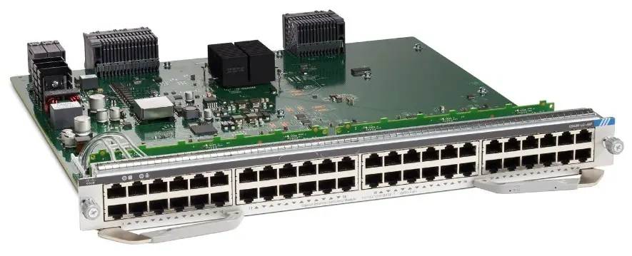
What is a Network Switch PCB and Why is Its Layout Important?
A network switch's functionality hinges on its Printed Circuit Board (PCB), which serves as the central nervous system connecting various components. This specialized board orchestrates how elements like Ethernet controllers, power regulation circuits, and network connectors interact, directly influencing the switch’s overall efficiency and data handling capabilities. The arrangement and interconnection of these parts on the PCB determine the switch’s ability to manage data traffic effectively.
A meticulously crafted PCB layout is crucial for ensuring peak performance in a network switch. It minimizes undesirable signal interference, optimizes power delivery, and facilitates robust, high-speed data transmission, often reaching or exceeding 1 Gigabit per second in contemporary devices. Conversely, a poorly conceived design can lead to problems such as signal crosstalk, electromagnetic interference (EMI), or excessive heat generation, all of which can severely compromise network stability and throughput. Adopting a methodical design approach helps in circumventing these issues, resulting in a product that performs optimally in today's demanding technological landscape.
Suggested Reading: Network Switch PCB Layout: A Comprehensive Design-to-Production Guide
Key Principles for Effective Network Switch PCB Design
Designing a circuit board for a network switch demands precise planning and adherence to established engineering best practices. Following core principles helps achieve superior performance and reliability.
Defining Project Requirements
Before commencing the design phase, it is vital to clearly outline the operational specifications of your network switch. Key considerations include the number of ports (e.g., 8, 16, 24), the required data transfer speeds (e.g., 1 Gbps or 10 Gbps), and specific power needs, such as Power over Ethernet (PoE) support. These specifications will dictate component selection and guide critical layout decisions. For example, a 24-port switch operating at 10 Gbps necessitates sophisticated high-speed signal routing and robust power management to handle the increased load. Understanding these details upfront aids in choosing appropriate materials and configuring the PCB's layer stack-up.
Optimizing Layer Stack-Up for Signal Integrity
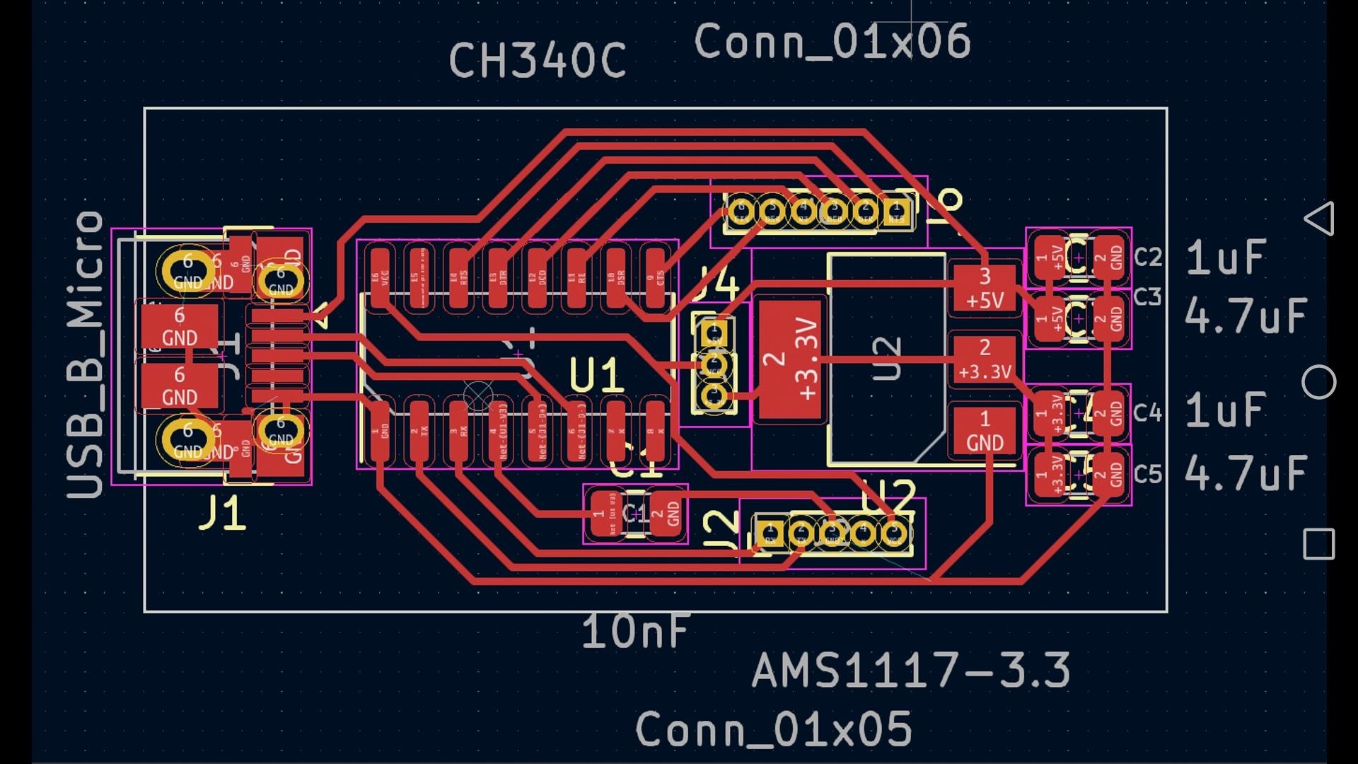
Given that network switches frequently process high-frequency signals, a well-engineered layer stack-up is paramount. A typical design might employ a 4 layers or 6 layers PCB, featuring distinct layers dedicated to power, ground, and signal routing. For instance, the top layer is often used for component placement and high-speed signal traces, while a dedicated ground plane helps reduce EMI and provides a stable reference for signals. A power plane ensures uniform power distribution, and additional routing or ground can be allocated to the bottom layer. It is critical to maintain controlled impedance for high-speed traces, commonly targeting 50 ohms for single-ended signals and 100 ohms for differential pairs, to prevent signal degradation.
Strategic Component Placement for Performance
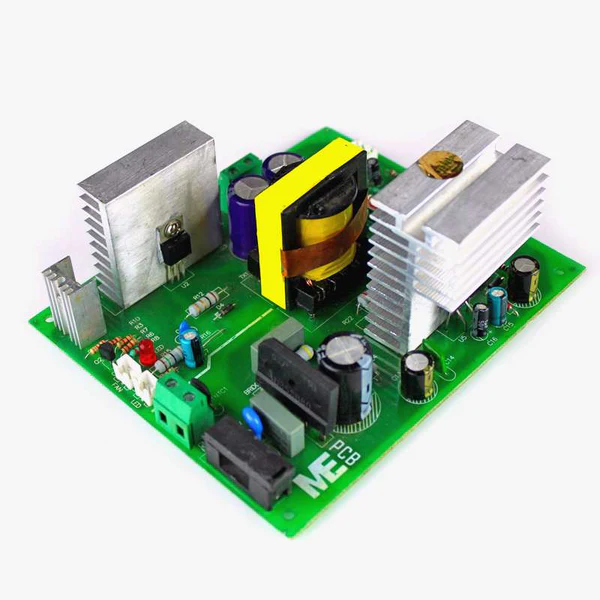
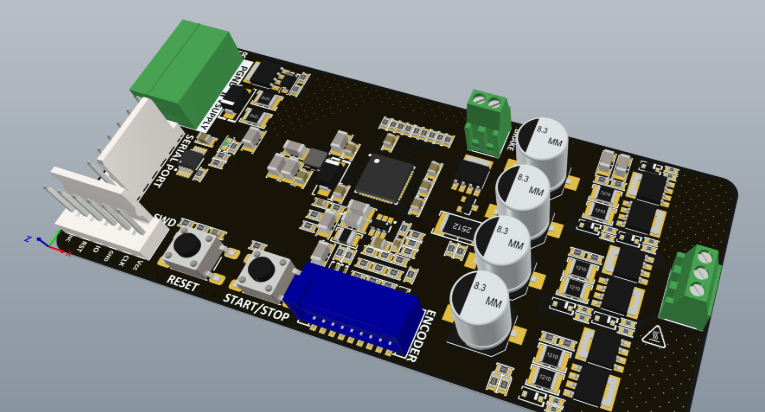
Components should be positioned logically to shorten trace lengths and minimize potential interference. Grouping related elements, such as Ethernet physical layer (PHY) chips near their corresponding RJ45 connectors, helps reduce signal delays. Power-related components, like voltage regulators, should be kept separate from sensitive signal areas to prevent noise coupling. Additionally, thermal management is a significant consideration. High-power components should be situated close to heat sinks or in well-ventilated zones to mitigate overheating, particularly in PoE-enabled switches where power dissipation can exceed 30 watts per port.
Routing High-Speed Signals Effectively
High-speed signals within network switches, such as those exchanged between the switch integrated circuit (IC) and Ethernet ports, demand meticulous routing. Best practices include avoiding sharp trace bends, instead utilizing 45-degree angles to lessen signal reflection. For differential pairs, maintaining equal trace lengths is critical to prevent timing skew, ideally keeping them within 5 mils (0.005 inches) of each other. Furthermore, traces should be routed away from noisy areas, such as power lines, to minimize crosstalk.
Stable Power Distribution and Decoupling
A consistent power supply is essential for network switches. Employ wide traces or dedicated power planes to accommodate current loads, particularly in PoE designs that might require up to 2 amperes per port. Placing decoupling capacitors, such as 0.1 μF ceramic capacitors, in close proximity to IC power pins (typically within 100 mils) helps filter noise and stabilize voltage levels, ensuring reliable operation.
The Manufacturing Pipeline for Network Switch PCBs
Once the design of your network switch PCB is complete, the subsequent phase is manufacturing, which transforms the digital design into a tangible circuit board ready for assembly. This process involves several critical stages.
Preparing Design Files
The initial step involves exporting comprehensive design files, including Gerber files, drill files, and a Bill of Materials (BOM). These documents contain all the necessary information for fabrication, detailing layer specifics, trace patterns, and component placements. Thoroughly checking for any potential errors, such as overlooked vias or incorrect pad dimensions, is crucial to prevent costly delays in production.
PCB Fabrication Steps
Fabrication is the process of constructing the bare PCB according to your design. Key stages include:
● Material Selection: Standard designs often use materials like FR-4, while high-speed switches may necessitate low-loss materials such as Rogers for improved signal integrity.
● Layer Lamination: Multiple board layers are carefully stacked and bonded together under controlled heat and pressure.
● Etching: Unwanted copper is selectively removed from non-conductive areas, forming the intricate patterns of traces and pads.
● Drilling: Precision holes are created for vias and through-hole components.
● Surface Finish: A protective coating, such as Hot Air Solder Leveling (HASL) or Electroless Nickel Immersion Gold (ENIG), is applied to prevent oxidation and ensure reliable solderability.

Rigorous Quality Assurance
Following fabrication, the PCBs undergo extensive testing to identify any manufacturing flaws. Electrical tests verify the absence of short or open circuits, while visual inspections confirm proper alignment and surface quality. For high-speed network switches, impedance testing is often performed to confirm that trace impedances meet specified values, such as 50 ohms, ensuring signal integrity.
Surface Mount Technology (SMT) Assembly for Network Switches
Surface Mount Technology (SMT) assembly is the predominant method for manufacturing modern network switch PCBs due to its efficiency and capacity to handle small, densely packed components.
Solder Paste Application and Component Placement
The process begins with applying solder paste, a precise mixture of tiny solder particles and flux, onto the PCB pads using a stencil. This ensures accurate placement for surface-mount components, including resistors, capacitors, and integrated circuits. Following this, automated pick-and-place machines precisely position components onto the solder paste. These machines can place thousands of components per hour, handling elements ranging from miniature 0402 resistors to complex Ball Grid Array (BGA) packages used for the main switch IC.
Reflow Soldering and Post-Assembly Inspection
The populated PCB then passes through a reflow oven, where controlled heat melts the solder paste, creating strong electrical connections between components and their respective pads. The typical peak temperature for lead-free solder is around 245°C, ensuring reliable joints without damaging sensitive components. After assembly, Automated Optical Inspection (AOI) systems thoroughly check for misaligned components or soldering defects. For critical network switch PCBs, X-ray inspection may be employed to verify connections beneath BGA packages. Finally, functional testing ensures the assembled board operates as designed, often involving rigorous data throughput tests at speeds of 1 Gbps or higher.
Integrating Through-Hole Technology in Network Switch PCBs
While SMT dominates contemporary designs, Through-Hole Technology (THT) remains relevant for network switch PCBs, particularly for components requiring superior mechanical strength, such as robust connectors and power inductors.
Component Insertion and Soldering
Through-hole components, characterized by their longer leads, are inserted into pre-drilled holes on the PCB. This insertion can be carried out manually for PCB prototype manufacturing runs or by automated machines for larger production volumes. Soldering these components is often performed using wave soldering, where the PCB traverses a wave of molten solder, typically at 260°C, which bonds the component leads to the pads. For smaller batches, hand soldering may be employed for greater precision.
Advantages and Trade-offs
Through-hole components provide exceptionally strong mechanical bonds, making them ideal for high-stress areas like RJ45 connectors in network switches, which experience frequent plugging and unplugging. However, they occupy more board space and their assembly process is generally slower compared to SMT, making them less suitable for high-density designs.
Addressing Challenges in Network Switch PCB Design
The design and manufacturing of network switch PCBs present specific challenges that require thoughtful solutions.
Maintaining Signal Integrity at High Speeds
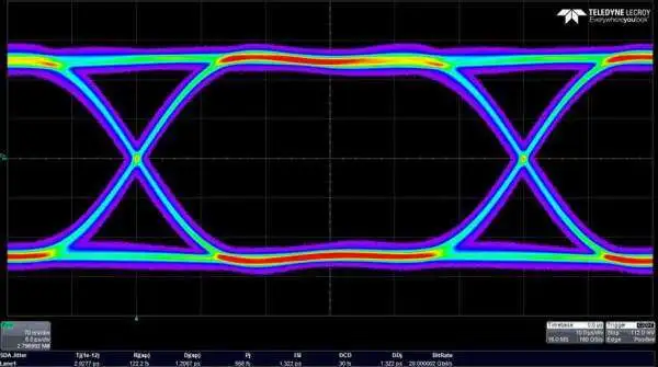
High data rates, such as 10 Gbps, can lead to issues like signal loss or crosstalk. These can be mitigated by implementing controlled impedance routing, utilizing appropriate termination resistors (e.g., 50 ohms), and keeping trace lengths as short as possible.
Effective Thermal Management
Network switches, especially those with Power over Ethernet (PoE), can generate substantial heat, with power dissipation sometimes exceeding 100 watts in certain designs. To manage this effectively, incorporate thermal vias, utilize heat sinks, and ensure adequate spacing around high-power components.
Mitigating EMI and Noise
Electromagnetic interference (EMI) can disrupt network performance. Employing comprehensive ground planes, shielding sensitive areas, and adhering to proper decoupling practices are essential steps to minimize unwanted noise.
Final Validation and Deployment Stages
Before moving to full-scale production, rigorous prototype testing is indispensable. This involves conducting stress tests that simulate real-world operational conditions, such as continuous data transfer at maximum capacity (e.g., all 24 ports operating at 1 Gbps). Critical performance metrics, including packet loss, latency, and power consumption, are measured to ensure the design meets all specified requirements.
Upon successful completion of testing, the project can transition to full-scale production, ideally with a trusted manufacturing partner. Maintaining clear communication regarding design files, assembly specifications, and quality benchmarks is paramount to prevent errors as production scales up.
Crafting a Robust Network Switch PCB: Concluding Thoughts
Developing a reliable network switch PCB layout demands meticulous attention at every phase, from initial design guidelines to manufacturing processes such as SMT assembly and through-hole technology. By consistently applying best practices for signal integrity, power distribution, and thermal management, engineers can produce devices that meet the rigorous demands of contemporary networking environments.
Whether the goal is to design a compact office switch or a robust industrial-grade solution, the principles discussed in this guide provide a strong foundation. With careful planning and precise execution, your network switch PCB will deliver uninterrupted connectivity and enduring reliability. Begin applying these insights to your upcoming projects to experience the transformative impact of a well-engineered PCB.