Introduction
In avionics systems, printed circuit boards (PCBs) handle critical signals that control flight operations, navigation, and communication. Electromagnetic interference (EMI) poses a severe threat by disrupting these signals, potentially leading to system malfunctions or safety risks. Avionics PCB EMI shielding becomes essential to maintain signal integrity in harsh electromagnetic environments, such as those near radars or high-power transmitters. Engineers must implement robust strategies to comply with stringent aerospace requirements and ensure reliable performance. This article explores proven EMI shielding strategies, focusing on grounding, shielding techniques, and filtering methods tailored for avionics applications. By understanding these approaches, designers can protect critical signals effectively.
Understanding Electromagnetic Interference in Avionics
Electromagnetic interference in avionics refers to unwanted electromagnetic energy that couples into PCB traces, degrading signal quality or causing false triggers. In avionics systems, EMI sources include onboard high-speed digital clocks, power converters, and external threats like lightning strikes or radio transmissions. Conducted EMI travels through power and ground lines, while radiated EMI propagates through the air and induces currents on PCB surfaces. These interferences can corrupt data in flight control units or navigation receivers, compromising aircraft safety. The high density of components on modern avionics PCBs amplifies susceptibility due to close proximity of sensitive analog and digital circuits. Addressing electromagnetic interference in avionics early in the design phase prevents costly redesigns and ensures compliance with performance standards.
PCBs in avionics operate under extreme conditions, including vibration, temperature cycles, and intense EMI fields, making mitigation non-negotiable. Poor EMI control leads to bit errors in digital signals or offset drifts in analog sensors. Engineers classify EMI by frequency: low-frequency magnetic fields couple via loops, while high-frequency electric fields affect trace capacitance. Quantifying EMI risks involves modeling field interactions during layout. Ultimately, avionics PCB EMI shielding strategies must balance weight, cost, and effectiveness for airborne applications.
Principles of EMI Generation and Propagation in Avionics PCBs
EMI generation on PCBs stems from rapid voltage or current changes creating time-varying fields that radiate or conduct away from sources. Clock edges in processors produce broadband noise, while switching regulators generate harmonics up to gigahertz ranges. Loop antennas formed by signal return paths amplify radiation, with larger loops emitting stronger fields. In avionics, shared power planes between noisy digital sections and sensitive RF receivers exacerbate crosstalk. Propagation occurs via capacitive coupling between parallel traces or inductive coupling through mutual inductance. Understanding these mechanisms guides targeted shielding interventions.
Field containment relies on minimizing current loop areas and providing low-impedance return paths close to signals. Without proper planes, fields extend far, coupling into adjacent circuits. Multilayer stackups with dedicated planes reduce impedance, confining fields between layers. Avionics designs often face mixed-signal challenges, where digital noise invades analog sections. Simulations reveal hotspots, but physical principles like Faraday's law underscore shielding needs. These fundamentals inform all avionics PCB EMI shielding practices.
Grounding for EMI Reduction in Avionics PCBs
Grounding forms the foundation of EMI mitigation by providing a low-impedance path for noise currents, preventing them from radiating. In avionics PCBs, a continuous ground plane on inner layers shields signals and returns currents directly beneath traces, minimizing loop areas. Splitting grounds between analog and digital domains, connected at a single point, avoids loops while isolating noise. Multiple vias stitching ground planes to surface layers enhance shielding effectiveness across frequencies. Engineers must avoid ground slots under signals, as they increase inductance and EMI radiation. Proper grounding for EMI reduction in avionics PCB aligns with IPC-2221 guidelines for controlled impedance and noise suppression.
Via fencing around high-speed traces connects ground planes, creating a Faraday cage effect that attenuates fields. In multilayer boards, dedicating layers to ground adjacent to signal layers tightens field coupling. Star grounding suits low frequencies, while plane grounding excels at high speeds common in avionics. Decoupling capacitors bridge power to ground near ICs, shunting high-frequency noise. Testing verifies ground integrity through impedance measurements. These techniques reduce emissions by orders of magnitude, ensuring clean signals.
Shielding Techniques for Avionics PCBs
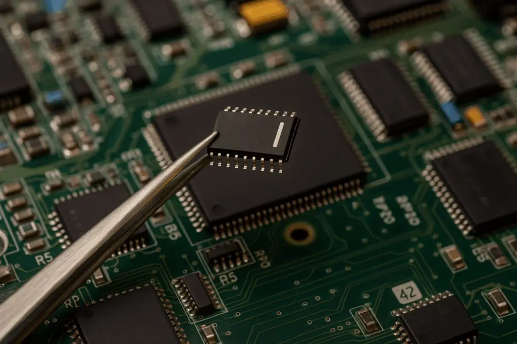
Shielding techniques for avionics PCBs block external fields and contain internal emissions using conductive barriers. Ground planes act as primary shields, reflecting electric fields and absorbing magnetic ones when thick enough. Board-level metal cans enclose noisy sections, grounded at multiple points for seam integrity. Conformal coatings with conductive particles provide lightweight shielding over components. In flexible sections of rigid-flex avionics boards, copper pours or films prevent flex-induced gaps. These methods comply with IPC-6012DS requirements for high-reliability boards in harsh environments.
Cavity shielding targets specific ICs, with lids soldered or clipped for reuse during prototyping. Multilayer enclosures stack absorption and reflection layers for broadband performance. Guard traces along signal edges, grounded frequently, divert stray fields. Aperture control minimizes slots in shields, as they resonate at quarter-wave frequencies. Integration during layout prevents post-assembly rework. Shielding effectiveness improves with lower sheet resistance materials, balanced against weight penalties in avionics.
Filtering EMI in Avionics PCBs
Filtering EMI in avionics PCBs suppresses conducted noise before it radiates or couples. Ferrite beads on power lines present high impedance to high frequencies while passing DC. Pi-filters combining capacitors and inductors attenuate harmonics near sources. Common-mode chokes target differential-mode noise rejection on cables interfacing PCBs. Placement close to entry points maximizes effectiveness, per IEC 61000 series for EMC immunity. Bypass capacitors across supplies decouple IC transients dynamically.
Feedthrough capacitors mount on enclosures, filtering signals penetrating shields. LC networks tailor cutoff frequencies to avionics clock rates. Simulation optimizes values without over-damping signals. Multi-stage filters handle wideband threats. Verification via spectrum analysis confirms attenuation. These filters complement shielding, achieving comprehensive protection.
Integrated Best Practices for Avionics PCB Design
Combine strategies for optimal results: start with stackup planning, placing ground planes adjacent to signals. Route high-speed traces over continuous planes, minimizing bends and vias. Separate power domains with planes to isolate noise. Component placement groups analogs away from digitals, with filters at boundaries. Thermal vias under power devices prevent hotspots aiding EMI. DFM checks ensure manufacturability without compromising shields.
Prototype testing in EMI chambers validates designs early. Iterate based on near-field scans identifying leaks. Documentation traces decisions to standards. Multidisciplinary reviews catch oversights. These practices yield PCBs passing certification with margin.
Conclusion
Avionics PCB EMI shielding demands a holistic approach integrating grounding, shielding techniques, and filtering to safeguard critical signals. Ground planes and via stitching reduce emissions fundamentally, while enclosures and filters handle residuals. Adhering to standards like IPC-6012DS ensures reliability. Designers prioritizing these strategies mitigate risks in electromagnetic-rich environments. Implementing them systematically enhances system robustness and safety.
FAQs
Q1: What are the primary causes of electromagnetic interference in avionics PCBs?
A1: Electromagnetic interference in avionics arises from switching transients in digital circuits, power supply ripple, and external sources like onboard radars. These generate radiated and conducted noise coupling into sensitive traces. Mitigation starts with layout segregation and plane design. Grounding for EMI reduction in avionics PCB prevents loops amplifying fields. Overall, understanding sources guides targeted avionics PCB EMI shielding.
Q2: How does grounding contribute to EMI reduction in avionics PCBs?
A2: Grounding for EMI reduction in avionics PCB uses solid planes to provide return paths, minimizing radiation loops. Continuous inner-layer grounds shield signals and absorb noise currents. Vias fence traces, enhancing containment. Avoid splits under signals to prevent inductance spikes. This aligns with design standards for low-impedance paths. Testing confirms effectiveness in high-frequency regimes.
Q3: What shielding techniques are most effective for avionics PCBs?
A3: Shielding techniques for avionics PCB include ground planes, metal cans over ICs, and conductive coatings. Planes reflect fields internally, cans block external threats. Ground multiple seams for integrity. Guard traces add localized protection. Balance weight with performance for flight applications. These ensure compliance in EMI-intensive environments.
Q4: How can filtering help in managing EMI on avionics PCBs?
A4: Filtering EMI in avionics PCB employs ferrites, capacitors, and chokes near noise sources. Pi-networks attenuate harmonics effectively. Common-mode filters handle cable ingress. Placement minimizes parasitics. Tune to system clocks for precision. Combined with shielding, they achieve robust immunity.
References
IPC-6012DS — Qualification and Performance Specification for Rigid Printed Boards for Space and Military Avionics Applications. IPC.
IPC-2221B — Generic Standard on Printed Board Design. IPC.
IEC 61000-4-3 — Electromagnetic Compatibility (EMC) - Part 4-3: Testing and Measurement Techniques - Radiated, Radio-Frequency, Electromagnetic Field Immunity Test. IEC.


