Why Are Flexible PCBs Essential for Modern Wearable Health Devices?
In the rapidly expanding field of wearable health technology, the ability to create adaptable electronic circuits is transformative. Whether you’re experimenting with flexible PCB DIY projects or delving into advanced wearable electronics design, mastering flex circuits opens up new possibilities for innovative health monitoring solutions. This comprehensive guide from AIVON explores sophisticated methods for developing flexible PCBs specifically for health-oriented wearables. It covers everything from selecting appropriate flex PCB materials to executing complex advanced PCB projects, providing the knowledge needed to turn concepts into functional devices.
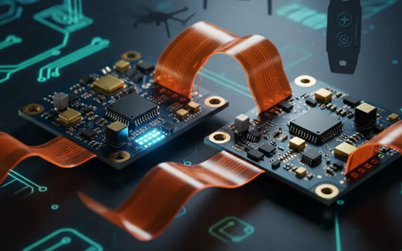
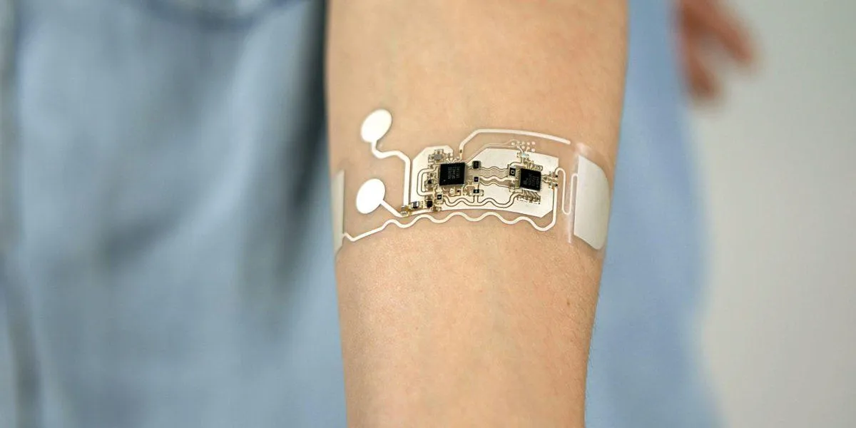
Flexible PCBs are distinct from their rigid counterparts because they are thin, light, and capable of bending and conforming to various shapes without compromising integrity. This pliability allows them to be integrated into compact, irregular spaces. For wearable health applications—such as fitness trackers, smartwatches, or medical patches—flexible PCBs are indispensable. They enhance user comfort by adapting to the body’s contours, reduce the overall weight of the device, and enable novel designs that are unachievable with rigid boards. The global wearable medical device market is experiencing significant growth, and flexible PCBs are central to this expansion, facilitating the creation of smaller, more robust, and user-friendly products.
What Materials Are Best for Flex PCBs in Wearable Health Technology?
The successful design of any flexible PCB hinges on selecting the right materials. These materials must offer a balance of flexibility, durability, and biocompatibility, as wearable health devices frequently make direct contact with the skin.
Key Material Considerations
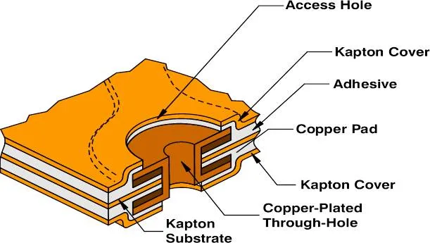
● Substrate Materials: Polyimide (PI) is the most prevalent substrate for flexible PCBs due to its exceptional thermal stability and inherent flexibility, tolerating temperatures up to 400°C, which is ideal for soldering. Polyester (PET) is a less expensive alternative, often used for applications with lower heat requirements.
● Conductive Layers: Copper is the industry standard for flex circuit traces, valued for its high conductivity and flexibility. Rolled annealed (RA) copper is preferred over electrodeposited (ED) copper because it offers superior flexibility and resistance to fatigue, which is crucial for devices that undergo repeated bending.
● Coverlay and Adhesives: A coverlay, typically made from polyimide with an adhesive layer, serves to protect the circuitry while maintaining the board’s flexibility. Biocompatible silicone-based adhesives are sometimes employed for direct skin contact applications.
● Surface Finishes: For wearable devices, surface finishes like immersion gold or organic solderability preservatives (OSP) are utilized to prevent oxidation and ensure reliable electrical connections. These finishes must also be non-toxic and safe for prolonged skin contact. When choosing materials, consider specific device requirements; for instance, a heart rate monitor might need materials that maintain high signal integrity, often targeting impedance values around 50 ohms.
What Are Crucial Design Aspects for Wearable Electronics?
Developing a flexible PCB for wearable electronics necessitates meticulous planning to ensure optimal functionality, longevity, and user comfort.
Essential Design Principles
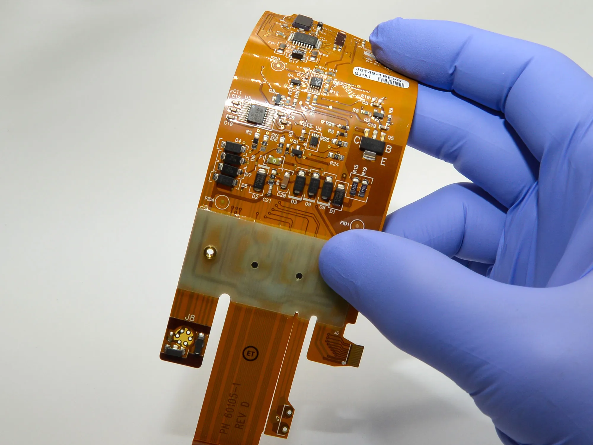
● Bend Radius and Flexibility Management: The bend radius, which is the smallest radius a flexible PCB can withstand without damage, is a critical parameter. A general recommendation is to maintain a minimum bend radius equivalent to at least 10 times the board's total thickness for dynamic (repeated) flexing. For example, a 0.1 mm thick board should have a bend radius of 1 mm or more. Exceeding this limit can cause trace cracking or delamination, so the design must account for the device's intended real-world use, such as a wristband that flexes continuously.
● Optimized Layer Stack-Up: For wearable applications, flexible PCBs typically range from 1 to 4 layers. Minimizing the number of layers helps maintain the board’s thinness and flexibility. Critical signal traces should be routed on inner layers for protection against mechanical stress, and staggered vias can be used to alleviate strain points. For high-speed signals in health sensors, maintaining controlled impedance, usually between 50-100 ohms, is vital.
● Strategic Component Placement: Components should be positioned in areas of the flex PCB that experience minimal bending or stress on solder joints. Opt for lightweight, low-profile surface-mount device (SMD) packages, such as 0201 or 0402, to reduce the overall bulk of the wearable design. For connectors or integrated circuits, reinforcing component areas with stiffeners might be necessary.
● Biocompatibility and Safety Standards: Given that wearable health devices come into direct contact with skin, all materials must be biocompatible and adhere to medical device standards like ISO 10993. It is crucial to avoid materials known to cause skin irritation or allergic reactions and to conduct long-term wear safety tests.
Related Reading: FR-4 PCB Design for Wearable Technology: Balancing Size, Weight, and Performance
What Advanced Techniques Enhance Flex Circuit Construction?
Building reliable flex circuits for wearable health applications involves employing sophisticated techniques that ensure both precision and durability.
Advanced Fabrication and Testing Approaches
● Simulation for Prototyping: Prior to physical manufacturing, leverage simulation software to evaluate your design for mechanical stress and signal integrity. These tools can predict the PCB’s behavior under bending and pinpoint potential failure areas. For example, simulating a 1 GHz signal speed for a health sensor ensures data accuracy and minimizes interference.
● Precision Etching for Fine Features: Wearable devices often require extremely fine traces (as small as 50 micrometers) to integrate complex circuitry into compact footprints. Advanced photo-etching processes are employed to achieve this high precision, ensuring clean edges and consistent trace widths for dependable signal transmission.
● Dynamic Flex Testing Protocols: After fabrication, subject the flexible PCB to rigorous dynamic flex testing. This process simulates real-world usage by cycling the board through its expected bend radius for at least 10,000 cycles to verify long-term durability. This is particularly critical for health devices like smart patches that must withstand constant movement.
● Integrated Sensor and Antenna Design: Many wearable health devices rely on embedded sensors (e.g., for temperature, heart rate) and integrated antennas for wireless communication. These components can be directly incorporated into the flex PCB to conserve space. Conductive inks or thin-film technologies can be used for antennas to maintain flexibility, targeting a 2.4 GHz signal range for common Bluetooth connectivity.
Tips for Flexible PCB DIY Projects by Hobbyists and Engineers
For those interested in flexible PCB DIY projects, constructing a flex circuit in a home lab or small workshop is achievable with the correct methodologies. While professional fabrication offers unparalleled precision, enthusiasts can begin with simpler designs using these tips:
Getting Started with DIY Flex Circuits
● Simple Design Focus: Start with a single-layer flexible PCB for a basic wearable, such as a step counter. Utilize open-source design software and aim for larger trace widths (e.g., 0.2 mm) to minimize etching errors.
● Accessible Materials: Source thin polyimide films and copper foil from online suppliers. These can be laminated using heat and pressure (e.g., with a household iron), then etched with a ferric chloride solution to create the trace patterns.
● Affordable Testing Tools: Use a multimeter to verify continuity and resistance (aiming for less than 1 ohm per trace) after etching. Manually flex the board to test its pliability, ensuring no cracks appear after 50-100 bends.
● Safety Precautions: Always wear gloves and work in a well-ventilated area when handling etching chemicals. Confirm that any DIY flex PCB materials intended for wearables are safe for skin contact. While DIY is excellent for learning, for complex or medical-grade wearable advanced PCB projects, partnering with a professional and large PCB manufacturer like AIVON ensures high-quality and reliable results.
Related Reading: Crafting Multi-Layer PCBs at Home: A Hobbyist’s Guide to Advanced Board Fabrication
What Are the Key Challenges in Flexible PCB Design for Wearables?
Designing flexible PCBs for health applications comes with a unique set of challenges. Recognizing these can help preempt costly errors:
● Signal Integrity Issues: Due to their thin structure, flex circuits are susceptible to noise and crosstalk. Employ ground planes and maintain adequate trace spacing (e.g., a minimum of 0.1 mm) to mitigate interference, especially for high-speed signals above 500 MHz.
● Durability Under Mechanical Stress: Repeated bending cycles can lead to fatigue failure. Reinforce high-stress areas with additional coverlay or adhesive layers to extend the product’s lifespan beyond 50,000 bend cycles.
● Cost Management: Flex PCBs typically incur higher production costs than rigid boards due to specialized materials and complex processes. Optimize your design by minimizing the number of layers and using standard material thicknesses (e.g., 0.05 mm polyimide) to control overall expenses.
Future Innovations in Flex PCBs for Wearable Health Technology
The horizon for flexible PCBs in wearable health tech is filled with exciting prospects. Emerging innovations include stretchable electronics, which allow circuits to elongate by up to 30% without damage. Conductive inks and advanced 3D printing techniques are also gaining traction, enabling fully customized, ultra-lightweight designs. Furthermore, the integration of AI-driven sensors into flex PCBs will facilitate real-time health data analysis with signal processing speeds exceeding 1 GHz.
AIVON is dedicated to remaining at the forefront of these technological advancements, offering state-of-the-art solutions for your advanced PCB projects. By harnessing these future trends, both hobbyists and professional engineers can establish themselves as leaders in wearable health innovation.
Related Reading: Flexible PCBs for Smart Eyewear: Design, Materials, and Assembly
Concluding Thoughts on Mastering Flexible PCBs for Wearable Health
Developing a flexible PCB for wearable health applications is a challenging yet highly rewarding endeavor that merges creative thinking with precise engineering. By comprehensively understanding flex PCB materials, mastering the nuances of wearable electronics design, and applying advanced techniques for building flex circuits, you can create groundbreaking devices that significantly enhance lives. Whether your focus is on flexible PCB DIY projects or more complex advanced PCB projects, the paramount considerations remain durability, biocompatibility, and user comfort.
AIVON is committed to supporting your journey with premium manufacturing services specifically tailored for flexible PCB requirements. Begin with modest designs, conduct frequent tests, and confidently scale your innovations. The future of wearable health technology is undeniably flexible—today is the day to redefine the boundaries of innovation!