Why is USB-C a Game-Changer for PCB Engineers?
The USB-C connector has dramatically transformed modern electronics through its compact, reversible design, capable of simultaneously delivering high-speed data, significant power, and extensive versatility. For engineers tasked with designing printed circuit boards (PCBs), incorporating USB-C connectors offers both significant opportunities and distinct challenges. A poorly executed USB-C integration can lead to signal degradation, power delivery inconsistencies, or even device malfunction, whereas a meticulously planned implementation ensures optimal reliability and performance.
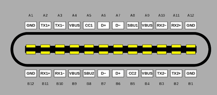
USB-C's growing prominence isn't solely about user convenience; it's fundamentally about its advanced capabilities. Supporting data transfer speeds up to 10 Gbps (USB 3.1 Gen 2), power delivery up to 100W, and compatibility with various protocols like HDMI and Thunderbolt, it represents a pivotal advancement. However, this power necessitates precision: its dense 24-pin configuration and high-frequency signals demand meticulous attention to detail in PCB design. Adhering to fundamental guidelines for USB-C integration is crucial for ensuring flawless project execution.
What Are the Key Design Aspects for USB-C Integration?
Successful USB-C integration on a PCB requires a focus on several critical areas, including maintaining signal integrity, managing power delivery effectively, and mitigating electromagnetic interference (EMI). Each of these elements plays a vital role in the overall performance and reliability of the final product.
Ensuring Pristine Signal Integrity
High-speed signals are fundamental to USB-C's performance, yet they are also vulnerable if not managed correctly. The USB 2.0 differential pair (D+ and D-) operates at 480 Mbps, while USB 3.1 SuperSpeed pairs (TX and RX) can reach up to 10 Gbps. To preserve signal integrity, several practices are essential:
● Controlled Impedance: Route differential pairs with a target impedance of 90 ohms (±10%) for USB 3.1 and 85 ohms for USB 2.0. Achieving this typically involves using a 4-layer PCB with a continuous ground plane directly beneath the traces.
● Length Matching: Keep the lengths of differential pair traces within 0.127 mm (5 mils) of each other to prevent timing skew, which is particularly critical for USB 3.1 given its rapid signal rise times.
● Minimizing Vias and Corners: Each via or sharp turn can introduce signal reflections. Limit vias to a maximum of two per differential pair and employ 45-degree bends instead of abrupt 90-degree angles.
Proper routing techniques significantly contribute to clean data transmission, thereby reducing bit errors and ensuring broad compatibility with connected devices.
Related Reading: Enhancing USB Performance: A Guide to Optimal PCB Layout and Signal Integrity
Managing Up to 100W Power Delivery
USB-C's Power Delivery (USB PD) specification allows for up to 20V at 5A, totaling 100W—a substantial increase over earlier USB standards. This capability necessitates robust power management:
● VBUS and GND Traces: Utilize wide traces (at least 0.5 mm for 3A, scaling up to 1.27 mm for 5A) to safely handle high currents without excessive voltage drop or heat generation. For a 5A design, a 1 oz copper layer typically requires a trace width of 1.0-1.27 mm to limit temperature rise.
● Decoupling Capacitors: Place 0.1 µF and 10 µF capacitors in close proximity to the VBUS pins (within 2.5 mm) to effectively filter noise and stabilize voltage fluctuations.
● CC Pin Configuration: The CC1 and CC2 pins are responsible for negotiating power roles. For a device acting as a basic power sink, connect 5.1 kΩ pull-down resistors to ground on both CC lines to signal 5V/3A capability to the power source.
A well-engineered power network is vital for preventing brownouts and ensuring safe, reliable operation under various load conditions.
Mitigating EMI and Ensuring Shielding
High-speed signals and switching power can generate electromagnetic interference (EMI), potentially disrupting adjacent circuits or violating regulatory standards. Effective mitigation strategies include:
● Ground Planes: Surround USB-C traces with a solid ground plane on adjacent layers. Avoid routing signals over splits or cutouts in the ground plane, as these can interrupt return paths and increase EMI.
● Shielding: Connect the USB-C connector's metal shell to the ground plane using multiple vias (at least four), spaced evenly around the connector footprint, to shunt noise effectively.
● Component Placement: Maintain a minimum distance of 1.27 mm (50 mils) between high-speed clocks, oscillators, or magnetic components and USB traces to prevent unwanted coupling.
Robust EMI control is essential for ensuring both regulatory compliance and the long-term reliability of your design in electromagnetically noisy environments.
What Are the Best Practices for USB-C PCB Layout?
Optimizing the physical layout of a USB-C connector and its associated traces on a fast turn PCB is crucial for achieving high performance and reliability. Strategic placement and routing minimize signal degradation and power issues.
Connector Placement and Mechanical Stability
Position the USB-C connector near the edge of the PCB to facilitate easy access for plugging and unplugging, while also minimizing the length of high-speed traces. For surface-mount connectors, ensure the footprint precisely matches the manufacturer's specifications—typically featuring a 0.5mm pin pitch and a 3.16mm receptacle width. Securing the connector with through-hole mounting tabs is recommended for enhanced mechanical stability, especially in devices that experience frequent connection and disconnection cycles.
Routing High-Speed Differential Pairs
Route USB 2.0 (D+/D-) and USB 3.1 (TX/RX) differential pairs as tightly coupled lines:
● Space traces within a pair 0.127-0.203 mm (5-8 mils) apart, and maintain at least 0.5 mm (20 mils) clearance from other signal traces to reduce crosstalk.
● Avoid routing traces underneath crystals, integrated circuits, or other components known to generate noise.
● Utilize length tuning techniques, such as serpentine traces, to match the lengths of traces within a pair, keeping any skew below 0.127 mm (5 mils).
Strategic Grounding and Layer Stackup
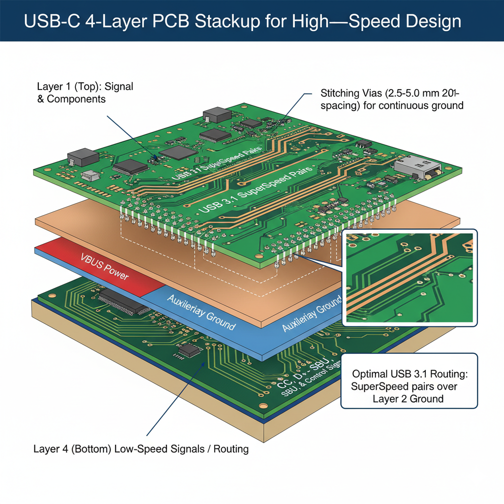
A 4 layer board stackup is generally considered ideal for USB-C designs due to its ability to provide clear signal isolation and robust grounding:
● Layer 1 (Top): Dedicated for signal traces and component placement.
● Layer 2: A solid ground plane, serving as a continuous reference for high-speed signals.
● Layer 3: Can be used as a power plane or an additional ground layer.
● Layer 4 (Bottom): Suitable for low-speed signals or less critical routing.
For USB 3.1, routing SuperSpeed pairs on the top layer directly over a ground plane on Layer 2 is optimal. This configuration minimizes impedance discontinuities and provides an efficient, low-inductance return path. Incorporate stitching vias along the edges of the traces every 2.5-5.0 mm (100-200 mils) to connect the ground planes across different layers, ensuring a continuous ground reference.
Related Reading: PCB Ground Planes – What are They and Why are They Important?
What Common USB-C Design Pitfalls Should Be Avoided?
Even with careful planning, several common issues can arise in USB-C PCB designs, potentially leading to performance problems. Awareness of these pitfalls and proactive measures can prevent costly rework.
Preventing Impedance Mismatches
An impedance mismatch, such as 100 ohms instead of the target 90 ohms, can cause signal reflections, severely degrading data transfer rates. Always use a PCB design tool equipped with an impedance calculator and cross-verify these calculations with your fabricator's specified layer stackup data. Prototype testing with a time-domain reflectometer (TDR) is highly recommended to confirm actual impedance values.
Avoiding Overheating Power Traces
Undersized VBUS traces, for instance, a 0.25 mm (10 mil) trace for a 5A current, risk overheating, which can lead to delamination or outright failure of the PCB. Calculate appropriate trace widths using IPC-2221 standards: for 1 oz copper carrying 5A, a trace width of at least 1.2 mm (47 mils) is typically required to keep temperature rise below 20°C. For designs pushing power limits, a thermal simulation can provide crucial insights.
Ensuring Robust ESD Protection
USB-C ports are frequently exposed to electrostatic discharge (ESD) events. Without adequate protection, an ESD strike of 15 kV can permanently damage sensitive integrated circuits. Incorporate ESD suppressors, such as TVS diodes rated appropriately for the VBUS voltage (e.g., 5V or 20V), positioned as close as possible to the connector pins (within 1.27 mm or 50 mils).
How to Validate Your USB-C PCB Design
Thorough testing is an indispensable step before proceeding to mass production, ensuring your USB-C PCB design meets performance expectations and reliability standards.
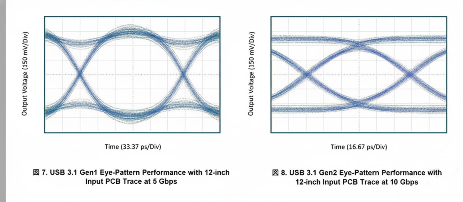
Comprehensive Signal Integrity Testing
Utilize an oscilloscope to analyze eye diagrams for both USB 2.0 and 3.1 signals. A "clean" eye diagram—typically characterized by more than 80% eye height and less than 20% jitter—serves as confirmation of signal compliance and quality.
Rigorous Power Delivery Evaluation
Conduct a load test on the VBUS line at its maximum intended current (e.g., 3A or 5A) and precisely measure the voltage drop. The measured voltage should remain within 5% of the specified value (e.g., a minimum of 4.75V for a 5V rail).
Compliance and Certification Checks
If your product is destined for commercial markets, undertaking USB-IF certification tests is critical. Specialized tools, such as the Ellisys USB Explorer, can automate this extensive testing process. Prototyping and iterative testing are invaluable for identifying and resolving issues early in the development cycle, ultimately saving both time and cost.
Partnering with AIVON for USB-C Integration Success
For engineers navigating the complexities of USB-C integration, collaborating with a knowledgeable PCB manufacturer is a distinct advantage. AIVON provides rapid PCB prototyping services, enabling design iterations and testing of signal routing or power adjustments within days rather than weeks. This swift turnaround supports agile development cycles.
AIVON's advanced manufacturing capabilities are specifically designed to meet the tight tolerances essential for USB-C's dense layouts, including features like 6-mil traces and 0.5mm-pitch footprints. Moreover, their efficient global logistics ensure that boards are delivered precisely where and when your project requires them, helping to keep your development timeline on track. Whether you are refining a high-speed data hub or a robust power sink, AIVON's expertise is instrumental in transforming your USB-C vision into a tangible, high-performing reality.
Concluding Thoughts on Robust USB-C Designs
Integrating USB-C connectors into your PCB designs unlocks a vast array of possibilities, offering high-speed data transfer, reliable power delivery, and broad universal compatibility. However, achieving success in this area is entirely dependent on precision: meticulously controlled impedance, thoughtful trace routing, and solid grounding are absolutely non-negotiable. By diligently adhering to these guidelines—such as maintaining tight differential pairs, appropriately sizing power traces, and effectively shielding against EMI—you will construct a design that is not only functional but also inherently reliable. Thorough testing and a proactive approach to avoiding common pitfalls will ensure your USB-C implementation stands up to the rigorous demands of real-world use.