What Defines a Network Switch PCB Layout and Why Is Its Design Critical?
A network switch PCB (Printed Circuit Board) layout forms the fundamental core of any network switch—a device engineered to interconnect multiple network components and efficiently direct data traffic. The precise arrangement and interconnection of essential components like Ethernet controllers, power regulators, and various connectors on this PCB directly influence the switch's overall performance, signal integrity, and long-term durability.
A meticulously designed network switch PCB layout guarantees minimal signal interference, optimized power distribution, and dependable high-speed data transfer, frequently surpassing 1 Gbps in contemporary switches. Conversely, a poorly executed design can lead to critical issues such as crosstalk, debilitating electromagnetic interference (EMI), or excessive overheating, all of which can severely compromise network performance. Adopting the correct design methodology allows you to circumvent these pitfalls and develop a product that excels in today’s rapidly evolving technological landscape.
What Are the Core Principles for Network Switch PCB Design?
Designing a PCB specifically for a network switch necessitates meticulous planning and strict adherence to a specialized set of guidelines. The following core principles are essential for achieving optimal results:
Understanding System Requirements
Before initiating any design work, it is paramount to thoroughly define the exact specifications of your network switch. Key factors to consider include the total number of ports (e.g., 8, 16, or 24 ports), the required data transfer speed (1 Gbps or 10 Gbps), and specific power demands (e.g., support for Power over Ethernet—PoE). These initial specifications will guide your subsequent component selection and all critical layout decisions. For instance, a 24-port switch designed to support 10 Gbps speeds will inherently demand advanced high-speed signal routing and robust power management capabilities to handle the substantial data load. Understanding these details upfront is crucial for selecting appropriate PCB materials and optimizing the layer stack-up.
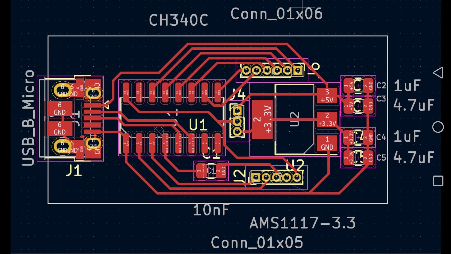
Optimizing Layer Stack-Up for Signal Integrity
Network switches routinely process high-speed signals, making a carefully planned layer stack-up absolutely critical. A typical design might employ a 4 layer or 6 layer PCB, featuring dedicated layers for power, ground, and signal routing. A common configuration might include: a top layer for components and high-speed signal traces; a ground plane to minimize EMI and provide a stable signal reference; a power plane for consistent power distribution to all components; and a bottom layer for additional routing or ground plane extension. It is imperative to ensure controlled impedance for all high-speed traces, often targeting 50 ohms for single-ended signals or 100 ohms for differential pairs, to prevent any degradation of signal quality.
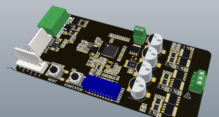
Efficient Component Placement
Strategically place components to minimize trace lengths and effectively prevent interference. Group related components together, such as positioning Ethernet PHYs in close proximity to RJ45 connectors, to reduce signal delays. Keep power-related components, like voltage regulators, physically separated from sensitive signal areas to avoid noise coupling. Furthermore, prioritize thermal management in your layout. High-power components should be positioned near designated heat sinks or ventilation zones to prevent overheating, a particularly critical consideration for PoE-enabled switches that can dissipate over 30W per port.
Routing High-Speed Signals
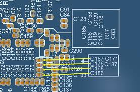
The high-speed signals within network switches, such as those connecting the switch IC to the Ethernet ports, demand exceptionally precise routing techniques. Adhere to these critical guidelines: avoid sharp 90-degree bends in traces, instead utilizing 45-degree angles to minimize signal reflections. Maintain exact equal trace lengths for all differential pairs, ideally within 5 mils (0.005 inches) of each other, to prevent timing skew. Keep these sensitive traces well away from noisy areas, such as power lines, to minimize unwanted crosstalk.
Power Distribution and Decoupling
A highly stable power supply is indispensable for the reliable operation of network switches. Utilize wide traces or dedicated power planes capable of handling significant current loads, especially for PoE designs which may require up to 2A per port. Position decoupling capacitors (e.g., 0.1 μF ceramic capacitors) in very close proximity to the IC power pins, typically within 100 mils of the pin, to effectively filter noise and maintain stable voltage levels.
The Manufacturing Journey of a Network Switch PCB
Once your network switch PCB layout design is finalized, the subsequent stage is manufacturing. This intricate process transforms your digital design into a tangible physical board, ready for component assembly. Here's an outline of the primary stages involved:
Design File Preparation and PCB Fabrication
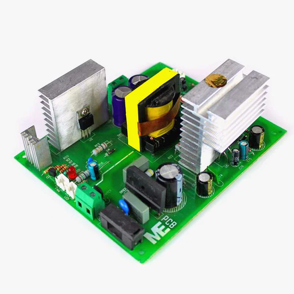
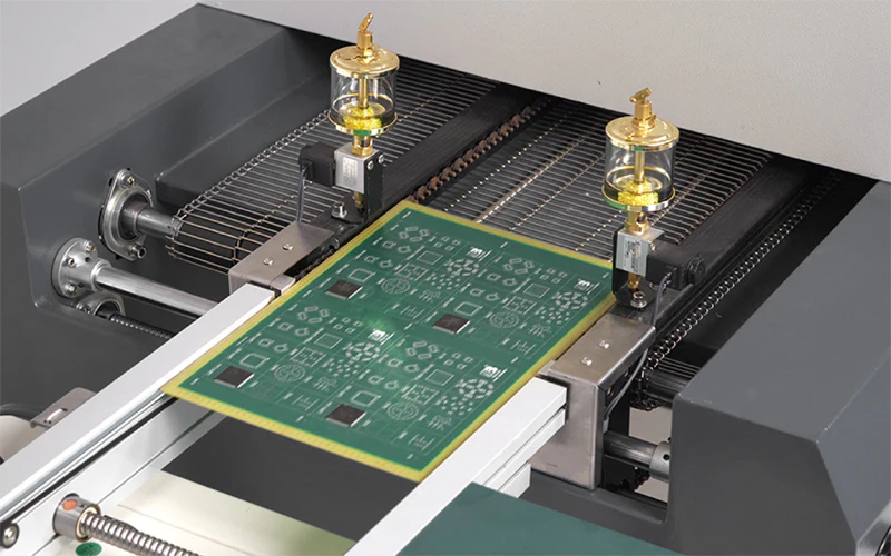
The first step is to accurately export all necessary design files, which include Gerber files, drill files, and a comprehensive Bill of Materials (BOM). These files encapsulate all the critical information required for fast turn PCB fabrication, such as detailed layer configurations, precise trace patterns, and exact component placements. It is crucial to meticulously double-check these files for any potential errors, such as missing vias or incorrect pad sizes, to prevent costly manufacturing delays. PCB fabrication involves the creation of the bare PCB according to your design. This process typically encompasses material selection (FR-4 for standard designs, or low-loss materials like Rogers for high-speed switches), layer lamination (multiple layers bonded under heat and pressure), etching (removal of copper from non-conductive areas), drilling (for vias and through-hole components), and application of a surface finish (e.g., HASL or ENIG) to prevent oxidation and ensure solderability.
Rigorous Quality Checks
Following fabrication, the bare PCB undergoes extensive testing for various defects. Electrical tests are performed to detect any shorts or open circuits, while visual inspections confirm proper alignment and surface quality. For high-speed network switches, impedance testing is often conducted to verify that critical traces meet specified values, such as 50 ohms.
Surface Mount Technology (SMT) Assembly for Network Switch PCBs
Surface Mount Technology (SMT) assembly is the predominant method for manufacturing modern network switch PCBs, valued for its efficiency and capability to handle small, high-density components. Here’s a breakdown of the typical workflow:
Solder Paste, Component Placement, and Reflow
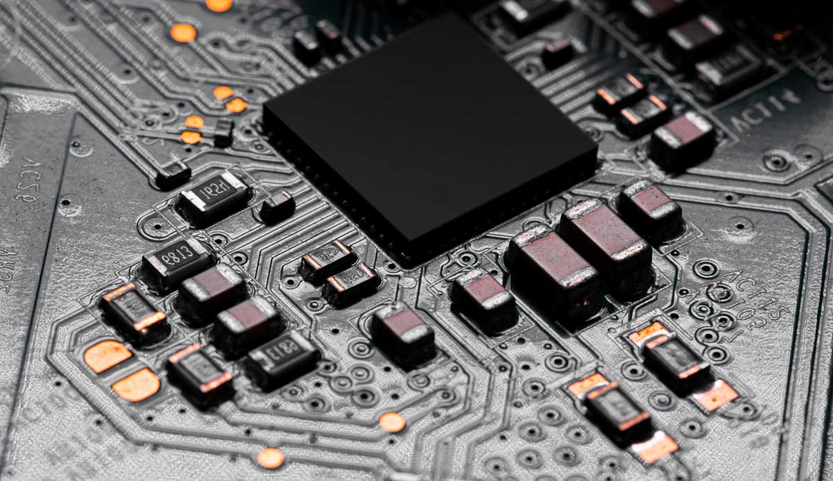
Solder paste, a precise mixture of minute solder particles and flux, is accurately applied to the PCB pads using a stencil. This ensures meticulous placement for all surface-mount components, including resistors, capacitors, and integrated circuits (ICs). Automated pick-and-place machines then precisely position these components onto the solder paste, often achieving placement rates of thousands of components per hour. For a network switch, this includes everything from tiny 0402 resistors to complex BGA (Ball Grid Array) packages for the main switch IC. The PCB subsequently moves through a reflow oven, where controlled heat melts the solder paste, creating robust electrical connections between the components and their respective pads. The temperature profile typically peaks around 245°C for lead-free solder, guaranteeing reliable joints without damaging sensitive components.
Post-Assembly Inspection and Testing
After the reflow soldering process, Automated Optical Inspection (AOI) systems thoroughly examine the PCB for any misaligned components or soldering defects. For critical network switch PCBs, X-ray inspection may be employed to verify the integrity of connections beneath BGA packages. Finally, comprehensive functional testing ensures that the assembled board operates precisely as intended, often involving rigorous data throughput tests at speeds of 1 Gbps or higher.
Integrating Through-Hole Technology in Network Switch PCBs
While SMT dominates contemporary designs, Through-Hole Technology (THT) remains relevant in network switch PCBs for components demanding superior mechanical strength, such as connectors and larger power inductors. Here’s an overview of its application:
Component Insertion and Soldering
Through-hole components, characterized by their longer leads, are carefully inserted into pre-drilled holes on the PCB. This process can be executed manually for prototype boards or through automated machinery for larger production volumes. Wave soldering is the prevalent method for attaching through-hole components. The PCB is passed over a wave of molten solder, typically at 260°C, which forms strong bonds between the component leads and the pads. For smaller production runs or specific precision requirements, hand soldering may also be utilized.
Advantages and Disadvantages
Through-hole components offer inherently strong mechanical bonds, making them ideal for high-stress components like RJ45 connectors in network switches that experience frequent plugging and unplugging cycles. However, a drawback is that they occupy more board space and their assembly process is generally slower compared to SMT, which makes them less common in high-density PCB designs.
Common Challenges and Solutions in Network Switch PCB Layout
Designing and manufacturing a network switch PCB inherently involves a unique set of challenges. Here are a few prevalent issues and their effective solutions:
Maintaining Signal Integrity at High Speeds
High-speed data rates, often reaching 10 Gbps, can lead to significant signal loss or undesirable crosstalk. To mitigate these issues, employ controlled impedance routing techniques, utilize appropriate termination resistors (e.g., 50 ohms), and keep critical trace lengths as short as possible.
Effective Thermal Management
Network switches, particularly those with Power over Ethernet (PoE) capabilities, can generate substantial amounts of heat, with power dissipation potentially exceeding 100W in certain designs. To manage this effectively, integrate thermal vias, utilize strategically placed heat sinks, and ensure ample spacing around all high-power components to facilitate heat dissipation.
Mitigating EMI and Noise
Electromagnetic interference (EMI) can severely disrupt network performance. To minimize noise, incorporate robust ground planes, shield sensitive areas of the PCB, and strictly adhere to proper decoupling practices for all power rails and ICs.
Final Steps: Rigorous Testing and Deployment
Before proceeding to mass production, extensive prototype testing is absolutely crucial. Conduct rigorous stress tests to accurately simulate real-world operating conditions, such as sustained data transfer at maximum capacity (e.g., all 24 ports operating at 1 Gbps simultaneously). Meticulously measure key performance metrics including packet loss, latency, and power consumption to confirm that the design fully meets all specified expectations.
Once all testing phases are successfully completed, transition to full-scale production with a trusted manufacturing partner. Ensure exceptionally clear and consistent communication regarding all design files, specific assembly requirements, and stringent quality standards to prevent any errors or inconsistencies during the scaling process.
Conclusion: Engineering Reliable Network Switch PCBs
The creation of a network switch PCB layout that delivers consistent reliability demands meticulous attention to detail at every stage—from the initial design guidelines through to advanced manufacturing processes such as SMT assembly and through-hole technology. By diligently applying best practices for ensuring signal integrity, optimizing power distribution, and implementing effective thermal management strategies, you can develop a product that not only meets but exceeds the demands of contemporary networking environments.
Whether your design objective is a compact office switch or a robust industrial-grade solution, the principles discussed in this guide provide an unwavering foundation. With careful planning and precise execution, your network switch PCB will deliver seamless connectivity and enduring reliability. Begin applying these insights to your next project today and experience the transformative impact of a professionally designed PCB!