Introduction
Telecommunications PCBs power routers, switches, and base stations. Assembly processes evolve from prototyping to mass production for reliability under constant signals. Prototyping tests designs quickly with small runs, while mass production scales for high volume with automated efficiency. SMT dominates for dense components, and through-hole PCB methods add mechanical strength for connectors. In my assembly experience, early DFM catches issues that save weeks later. Cost pressures demand seamless transitions. This article shares practical steps for telecom applications, covering techniques, challenges, and fixes from line-floor insights. Engineers learn to balance speed and quality. Keywords like PCB assembly guide selections for high-frequency boards. These strategies ensure uptime in networks.
What Is Telecommunications PCB Assembly and Why It Matters
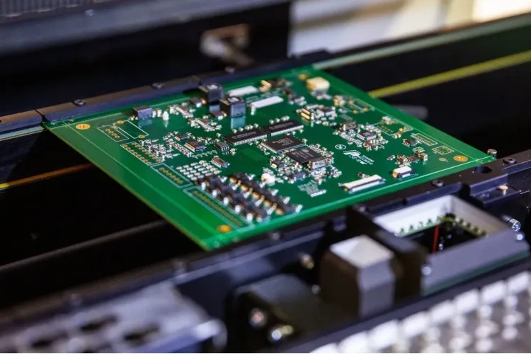
Telecommunications PCB assembly joins components to boards for signal routing. It spans prototyping for validation to mass production for deployment. Prototyping uses low volumes to verify functionality, while PCB mass production ramps to thousands of units with yield targets over 98 percent.
SMT places surface-mount parts via reflow, and through-hole PCB inserts leads for wave soldering. Telecom often demands mixed technology for RF modules and power pins. Signal integrity suffers from poor joints; failures disrupt calls or data streams. In 5G-era networks, boards handle gigahertz frequencies and heat from amplifiers. IPC-A-610H sets Class 3 criteria for high-reliability telecom assemblies. Compliance prevents field returns. Prototyping spots EMI early, while mass production optimizes cost per unit. Mismatched assembly that skips prototyping can lead to 25 percent rework in volume.
| Stage | Volume | Key Process | Focus Area |
|---|---|---|---|
| Prototyping | 1–100 | Hand/Semi-auto | Functionality test |
| Mass Production | 1000+ | Full automation | Yield and cost |
Technical Principles of PCB Assembly in Telecom
Assembly principles center on solder joints and component alignment. The telecommunication PCB uses FR4 or Rogers laminates for low loss, with layer counts up to 16 for backplanes.
SMT Principles
SMT applies solder paste, places parts, then reflows. Stencils cut apertures for 100-micron deposits. Placement accuracy reaches 25 microns for BGAs. Reflow profiles peak at 245°C for lead-free. IPC-J-STD-020E classifies moisture sensitivity to prevent popcorning. Thermal vias under ICs manage heat, and current densities stay below 1 amp/mil for traces. Signal paths are minimized to curb crosstalk.
Through-Hole PCB Principles
Through-hole drills holes, inserts leads, then wave solders. Pins provide mechanical strength for edge connectors. Wave pots maintain 250°C flux. IPC-A-610H inspects hole fill over 75 percent. Mixed boards combine both SMT and through-hole techniques for passives, heatsinks, and RF sections. Principles ensure impedance control at 50 ohms. Profile tweaks can cut voids by 15 percent.
Practical Solutions and Best Practices
Shift from prototyping to mass production with phased scaling. Start with hand soldering for prototypes, then move to automated lines for high-volume production.
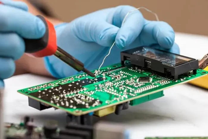
Prototyping Best Practices
Use jigs for repeatable placement, test with flying probes per IPC-TM-650, bake boards at 125°C to remove moisture, and select HASL finish for easy rework. Document anomalies in logs. Verify eye diagrams early to detect timing issues.
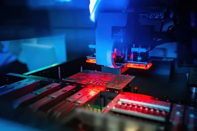
Mass Production Solutions
Implement SMT lines with dual feeders, optimize stencil thickness to 125 microns, and run AOI post-placement. Through-hole waves follow flux dip; post-solder cleaning removes residues. Yield tracking uses SPC charts. Additional best practices include DFM reviews (0.4 mm minimum spacing), panelization with breakaway tabs (fit 12 per 18-inch panel), traceability via bar-coded lots, and 100% functional testing for telecom.
| Process | Prototyping Tool | Mass Production Tool |
|---|---|---|
| Placement | Manual tweezers | Pick-and-place |
| Soldering | Hot air station | Reflow/wave oven |
| Inspection | Visual microscope | Automated X-ray |
Suggested Reading: From Prototype to Production: Scaling with Quick Turn PCB Manufacturing
Troubleshooting Insights from Assembly Lines
High-speed signals amplify joint flaws. Bridging in SMT arrays from excess paste can be fixed by reducing stencil volume to 90% and validating prints under a microscope. Through-hole PCB voids may arise from flux starvation; stirring wave pots every 30 minutes and pre-heating leads to 100°C aids hole fill. Thin proto pcb boards may warp under component weight; support fixtures in reflow prevent bowing. EMI in backplanes is mitigated by stitching ground planes around signals. BGA defects like head-in-pillow are resolved via IPC-7095D drag soldering techniques. Mass production delays often stem from feeder jams; regular nozzle calibration prevents them.
Conclusion
Telecommunications PCB assembly bridges prototyping innovation to mass production reliability. SMT enables dense component placement, while through-hole PCB ensures durability. Practical flows from hand to automated lines optimize outcomes. Troubleshooting refines yields for 5G and high-frequency demands. Experience proves phased approaches pay off, ensuring seamless telecom deployments. Future boards increasingly leverage AI for inspection and quality assurance.
FAQs
Q1: How does PCB assembly differ in prototyping versus mass production for telecom?
A1: Prototyping relies on manual SMT and through-hole techniques for quick iterations, while mass production automates for volume. Prototypes test signal paths, hot-air soldering handles fixes, and IPC-A-610H ensures uniform standards. Full-scale production uses reflow ovens for efficiency and reduced errors.
Q2: What role does SMT play in telecommunications PCB assembly?
A2: SMT mounts fine-pitch parts for dense telecom boards, supporting high-frequency routing. Paste printing and reflow form reliable joints, preventing crosstalk. Through-hole complements SMT for power and mechanical strength, ensuring robust router and base station assemblies.
Q3: Why include through-hole PCB in mass production for telecom applications?
A3: Through-hole provides durable connections for antennas, heatsinks, and edge connectors. It withstands vibrations in base stations, and wave soldering reliably fills vias. Prototypes verify pin fits early, reducing pull-out failures in mass production.
Q4: How to optimize prototyping for smooth mass production in PCB assembly?
A4: Conduct DFM audits for spacing and finishes, test thermal profiles, scale panelization gradually, and track defects. Unified fluxes for SMT and through-hole improve yields by up to 20%, preparing telecom boards for high-volume 5G production.
References
IPC-A-610H — Acceptability of Electronic Assemblies. IPC, 2019.
IPC-J-STD-020E — Moisture/Reflow Sensitivity Classification for Nonhermetic Surface Mount Devices. IPC/JEDEC, 2014.
IPC-7095D — Design and Assembly Process Implementation for BGAs. IPC, 2014.
IPC-TM-650 — Test Methods Manual. IPC, various sections, latest revisions.


