Introduction
Rigid-flex PCB stack-up design is a critical aspect of modern electronics, blending the durability of rigid boards with the adaptability of flexible circuits. This hybrid approach is essential for applications in aerospace, medical devices, and consumer electronics where space constraints and reliability are paramount. For electrical engineers, mastering stack-up design ensures optimal performance, structural integrity, and manufacturability. This article provides four professional tips focusing on anchoring techniques, maintaining structural integrity, utilizing blind and buried vias, and strategies to reduce PCB design complexity. By following these guidelines, engineers can address common challenges and enhance the functionality of their rigid-flex designs while adhering to industry standards.
What Is Rigid-Flex PCB Stack-up and Why It Matters
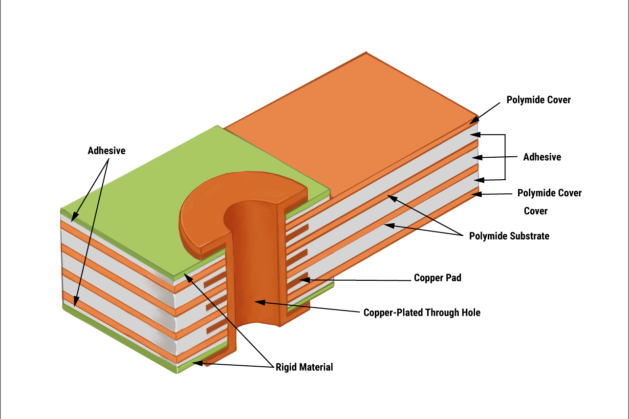
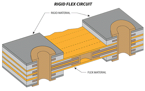
A rigid-flex PCB stack-up integrates rigid and flexible layers into a single unit, allowing the board to bend in specific areas while maintaining stability in others for component mounting. This design is crucial for devices requiring compact packaging and dynamic movement, such as wearable technology and foldable electronics. The stack-up defines the arrangement of conductive and insulating layers, impacting signal integrity, thermal management, and mechanical strength. A well-planned stack-up ensures reliable performance under stress, minimizes electromagnetic interference, and supports high-density layouts. For electrical engineers, understanding stack-up design is vital to balance electrical requirements with mechanical constraints, ensuring the final product meets both functional and durability expectations.
Technical Principles of Rigid-Flex PCB Stack-up Design
The design of a rigid-flex PCB stack-up involves several engineering principles to achieve a robust and efficient layout. The primary focus is on layer arrangement, material selection, and via integration to support both electrical and mechanical needs. Rigid sections often use FR4 or similar materials for strength, while flexible areas utilize polyimide for its bending capability. The transition zones between rigid and flex areas are critical, as they experience significant stress during bending. Proper alignment of layers prevents delamination and maintains signal continuity across these zones.
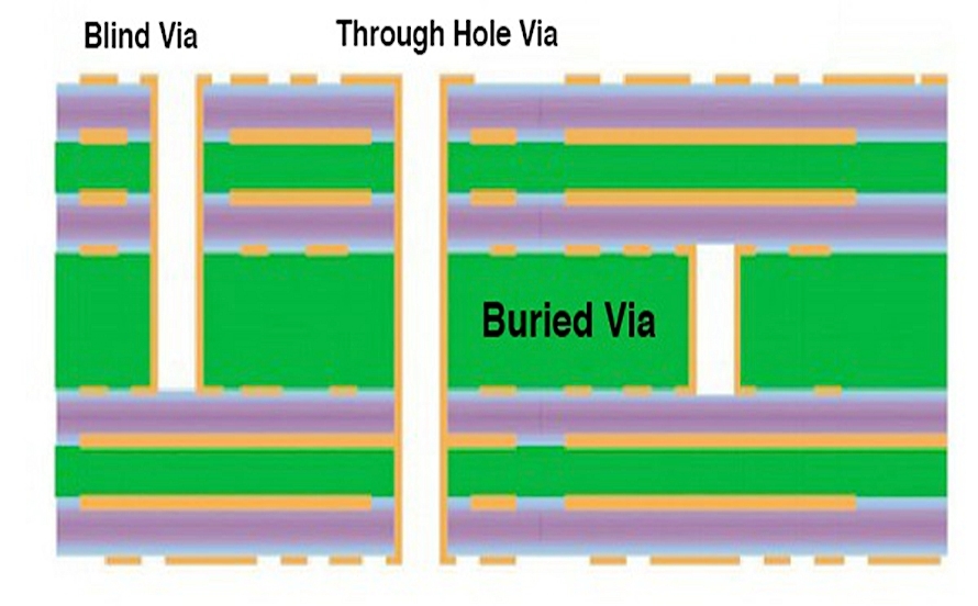
Vias play a key role in connecting layers, with blind and buried vias offering solutions for high-density designs. Blind vias connect an outer layer to an inner layer without passing through the entire board, while buried vias link internal layers only. These via types save space and improve routing efficiency but require precise manufacturing to avoid defects. Additionally, the stack-up must account for impedance control by maintaining consistent dielectric thickness and copper trace widths, especially for high-speed signals. Adhering to recognized standards ensures these principles are applied correctly for reliable outcomes.
Related Reading: The Impact of Impedance Control on Signal Integrity in High Speed Rigid Flex PCB Assembly
Pro Tip 1: Enhance Anchoring for Reliable Transitions
Anchoring is a fundamental technique to secure the flexible sections of a rigid-flex PCB to the rigid areas, preventing movement or stress-induced failures. Effective anchoring ensures the flex portion remains stable during bending, avoiding cracks or layer separation at transition points. One approach is to extend the rigid material slightly into the flex area, creating an overlap that reinforces the joint. This overlap distributes stress more evenly across the interface.
Another method involves using adhesive materials or additional copper features at the transition zone to lock the layers in place. Engineers should also consider the bend radius in these areas, ensuring it aligns with material capabilities to prevent tearing. Following guidelines from standards like IPC-2223C, which covers design rules for flexible circuits, helps in determining appropriate anchoring methods. By prioritizing robust anchoring, designers can significantly improve the longevity and reliability of their rigid-flex boards under dynamic conditions.
Pro Tip 2: Prioritize Structural Integrity in Stack-up Planning
Structural integrity is paramount in rigid-flex PCB design to withstand mechanical stress, thermal expansion, and environmental factors. A key factor is the symmetry of the stack-up, which balances stresses across layers to prevent warping or twisting. For instance, placing flexible layers centrally with rigid layers on the outer sides can help distribute bending forces evenly. Material selection also impacts integrity, with polyimide offering flexibility and FR4 providing rigidity where needed.
Related Reading: Beyond FR 4: Exploring Advanced Substrates for Rigid Flex PCB Assembly
Engineers must avoid abrupt changes in layer thickness at transition zones, as these can create weak points prone to cracking. Gradual transitions or stepped layer designs reduce stress concentration. Additionally, ensuring proper copper balance across layers minimizes uneven thermal expansion during operation. Adhering to IPC-6013D, which specifies performance requirements for flexible and rigid-flex boards, provides a framework for maintaining structural integrity. A robust design not only enhances durability but also supports consistent electrical performance over time.
Pro Tip 3: Leverage Blind and Buried Vias for High-Density Layouts
Blind and buried vias are essential tools for optimizing space in rigid-flex PCB designs, particularly in high-density applications. Blind vias connect surface layers to inner layers without penetrating the entire board, while buried vias link internal layers only, remaining invisible from the surface. These via types allow for more compact routing, freeing up space for additional components or traces. They are especially useful in rigid-flex designs where space is limited due to folding or bending requirements.
However, implementing these vias requires careful planning to ensure manufacturability. Precise drilling and plating processes are necessary to maintain connection reliability, as misalignment can lead to open circuits. Engineers should consult standards like IPC-6012E for guidance on via formation and inspection criteria. While blind and buried vias increase design density, they also add manufacturing complexity, so their use should be justified by specific layout needs. When applied correctly, they significantly reduce PCB design clutter and enhance signal routing efficiency.
Pro Tip 4: Reduce PCB Design Complexity with Simplified Stack-ups
Simplifying the stack-up is a practical strategy to reduce PCB design complexity, minimizing errors and improving manufacturability in rigid-flex boards. One effective method is to limit the number of layer transitions between rigid and flex sections, as each transition introduces potential failure points. Engineers can achieve this by grouping signals that require similar routing paths, reducing the need for excessive layer changes. This approach also streamlines the design process and lowers production costs.
Another tactic is to standardize via types and sizes wherever possible, avoiding a mix of through-hole, blind, and buried vias unless absolutely necessary. Consistent dielectric materials and thicknesses across layers further simplify impedance calculations and manufacturing steps. Following design guidelines from IPC-A-600K ensures acceptability criteria are met without overcomplicating the layout. By focusing on simplicity, engineers can create designs that are easier to fabricate, test, and maintain, ultimately leading to more reliable products with fewer design iterations.
For more knowledge about flexible and rigid-flex PCBs, see our comprehensive guide: Flexible and Rigid-Flex PCBs: The Complete Engineering Guide
Practical Insight: Balancing Design Goals with Manufacturability
Achieving an optimal rigid-flex PCB stack-up often involves balancing ambitious design goals with practical manufacturing constraints. For instance, while blind and buried vias enable high-density layouts, they can increase production time and cost due to specialized processes. Similarly, intricate anchoring techniques enhance structural integrity but may require advanced fabrication capabilities. Electrical engineers must collaborate closely with fabrication teams during the design phase to align on feasible specifications.
A useful practice is to simulate the stack-up under expected mechanical and thermal conditions using software tools compliant with industry standards. This step helps identify potential weak points, such as stress concentrations at flex zones, before physical prototypes are built. Iterative testing based on standards like IPC-6013D ensures the design meets performance criteria without over-engineering. By prioritizing both innovation and manufacturability, engineers can develop rigid-flex PCBs that perform reliably in real-world applications while remaining cost-effective to produce.
Conclusion
Rigid-flex PCB stack-up design is a complex but rewarding process that demands attention to anchoring, structural integrity, via selection, and design simplicity. By implementing the four professional tips outlined, electrical engineers can create robust designs that meet the demands of modern electronics. Effective anchoring secures transition zones, while balanced stack-ups ensure structural integrity under stress. Utilizing blind and buried vias optimizes space in dense layouts, and simplifying the design reduces PCB design complexity. Adhering to established industry standards guarantees reliability and manufacturability, paving the way for successful project outcomes in challenging applications.
FAQs
Q1: How does anchoring improve the reliability of rigid-flex PCBs?
A1: Anchoring strengthens the connection between rigid and flexible sections, preventing separation or cracking during bending. It distributes stress evenly at transition zones, enhancing durability. Techniques like material overlap or adhesive reinforcement ensure stability. Following standards like IPC-2223C helps engineers apply anchoring effectively for long-term reliability in dynamic applications.
Q2: Why is structural integrity critical in rigid-flex PCB stack-up design?
A2: Structural integrity ensures the PCB withstands mechanical stress, thermal changes, and environmental factors without failure. A balanced stack-up prevents warping, while proper material choices support durability. Standards like IPC-6013D guide engineers in maintaining integrity, ensuring the board performs reliably over time in demanding conditions.
Q3: What are the benefits of using blind and buried vias in rigid-flex designs?
A3: Blind and buried vias save space by enabling high-density routing in rigid-flex PCBs, ideal for compact layouts. They connect specific layers without occupying unnecessary board area, improving design efficiency. However, precise manufacturing per IPC-6012E is essential to avoid defects, making them a powerful tool when used strategically.
Q4: How can engineers reduce PCB design complexity in rigid-flex stack-ups?
A4: To reduce PCB design complexity, engineers should minimize layer transitions, standardize via types, and use consistent materials. Simplifying the stack-up lowers error risks and eases manufacturing. Adhering to IPC-A-600K ensures acceptability without overcomplicating layouts, resulting in designs that are efficient to produce and maintain.
References
IPC-2223C - Sectional Design Standard for Flexible/Rigid-Flex Printed Boards. IPC, 2016.
IPC-6012E - Qualification and Performance Specification for Rigid Printed Boards. IPC, 2020.
IPC-6013D - Qualification and Performance Specification for Flexible/Rigid-Flex Printed Boards. IPC, 2017.
IPC-A-600K - Acceptability of Printed Boards. IPC, 2020.


