Introduction
In the realm of printed circuit board (PCB) manufacturing, achieving high quality via plating is a critical factor for ensuring reliable electrical performance and structural integrity. Stacked vias, often used in high density interconnect (HDI) designs, present unique challenges in obtaining uniform copper deposition. Poor plating quality can lead to defects such as voids, insufficient thickness, or uneven coverage, which compromise signal integrity and board durability. This article explores the best practices for plating stacked vias, focusing on techniques to ensure consistent copper deposition. Aimed at electrical engineers, the content delves into the technical principles behind plating defects and offers practical solutions for optimizing the process in PCB manufacturing. Understanding these methods can significantly enhance the reliability of complex multilayer boards.
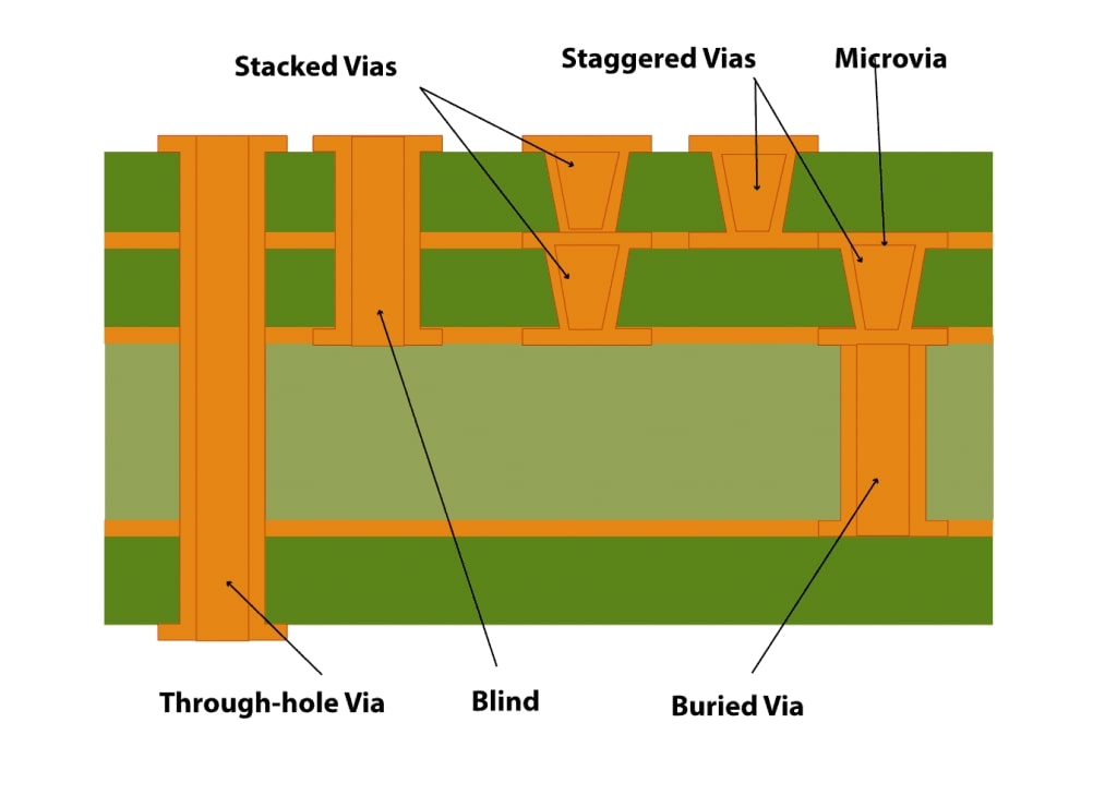
What Are Stacked Vias and Why Do They Matter
Stacked vias are vertical interconnects placed directly on top of one another across multiple layers of a PCB, commonly employed in HDI PCB designs to save space and improve routing density. Unlike staggered vias, which are offset, stacked vias require precise alignment and robust plating to maintain electrical continuity. Their importance lies in enabling compact designs for modern electronics, where space constraints are a constant challenge. However, the complexity of plating stacked vias increases the risk of defects, such as incomplete copper deposition or structural weaknesses at the via interfaces. Ensuring plating quality directly impacts the board's performance, especially in high frequency or high reliability applications. Addressing these challenges during PCB manufacturing is essential for meeting stringent industry standards and preventing costly failures in the field.
Related Reading: Stacked Vias in HDI PCBs: Design, Manufacturing, and Reliability
Technical Principles of Via Plating in Stacked Structures
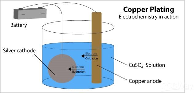
Via plating involves depositing a layer of copper inside drilled holes to create conductive pathways between PCB layers. The process typically includes electroless copper deposition as a seed layer, followed by electrolytic plating to build up the desired thickness. In stacked vias, the aspect ratio, which is the ratio of via depth to diameter, often becomes more challenging due to multiple stacked holes. High aspect ratios can hinder uniform copper deposition, as the plating solution struggles to penetrate deep into narrow vias.
One key principle is the throwing power of the plating solution, which refers to its ability to deposit copper evenly across all surfaces, including deep within vias. Poor throwing power results in thinner copper near the center of the via wall, creating weak points. Additionally, gas bubbles or contaminants trapped in the via can cause voids, disrupting conductivity. Temperature, current density, and solution agitation also play critical roles in determining plating quality. If these parameters are not controlled, defects such as nodules or overplating at via entrances can occur, affecting both electrical and mechanical properties.
For stacked vias, the alignment between layers adds another layer of complexity. Misalignment can create uneven surfaces or stress points, further complicating uniform deposition. Industry standards, such as IPC-6012E, outline specific requirements for via plating thickness and quality to ensure reliability. Understanding these technical factors is the foundation for mitigating plating defects in PCB manufacturing.
Common Plating Defects in Stacked Vias
Several plating defects can arise during the manufacturing of stacked vias, each with distinct causes and implications. Identifying these issues is crucial for implementing corrective measures. Below are the most prevalent defects encountered in via plating:
- Voids: These are empty spaces within the copper layer, often caused by trapped gas or poor solution flow. Voids reduce conductivity and weaken the via structure.
- Insufficient Thickness: Thin copper layers, especially in high aspect ratio vias, fail to meet minimum thickness requirements, leading to high resistance or breakage.
- Nodules: Excessive copper buildup at via openings, due to uneven current distribution, can interfere with layer stacking or component mounting.
- Cracks: Stress from thermal expansion or mechanical handling can cause cracks in the plated copper, particularly at the interface of stacked vias.
- Delamination: Poor adhesion between copper layers and the via wall, often due to contamination or inadequate surface preparation, results in separation over time.
These defects not only affect electrical performance but also compromise the board's ability to withstand environmental stresses. Standards like IPC-A-600K provide detailed acceptance criteria for identifying and classifying such defects during quality control inspections.
Best Practices for Achieving Uniform Copper Deposition
Optimize Via Design Parameters
Design plays a pivotal role in plating quality. Limiting the aspect ratio of vias ensures better solution penetration during plating. A lower aspect ratio, ideally below 10:1 as suggested by common industry practices, facilitates uniform copper deposition. Additionally, ensuring proper alignment of stacked vias during layout minimizes stress and uneven surfaces. Specifying adequate annular ring dimensions also supports consistent plating around via openings.
Control Plating Process Parameters
During electrolytic plating, maintaining optimal current density is essential. Too high a current can cause nodules, while too low a current results in insufficient thickness. Adjusting the plating bath temperature and agitation improves solution flow, enhancing throwing power. Regular monitoring and maintenance of the plating solution chemistry prevent contamination, which can lead to voids or poor adhesion.
Use Advanced Plating Techniques
Employing pulse plating, a method that alternates current on and off, can improve copper distribution in high aspect ratio vias. This technique reduces the risk of overplating at via entrances and promotes even deposition deeper within the structure. Additionally, ensuring a high quality electroless copper seed layer sets a strong foundation for subsequent electrolytic plating.
Implement Rigorous Surface Preparation
Before plating, thorough cleaning and desmearing of via walls remove drilling residues and contaminants. This step enhances copper adhesion and prevents delamination. Activating the surface with a proper catalyst during electroless plating also ensures a uniform initial layer, critical for stacked via reliability.
Adhere to Industry Standards
Compliance with standards such as IPC-6012E for performance specifications and IPC-A-600K for acceptability criteria is non-negotiable. These guidelines define minimum plating thickness, typically around 20 to 25 micrometers for most applications, and outline defect classification to ensure consistent quality. Regular inspections using microsectioning and automated optical inspection help verify compliance.
Monitor and Mitigate Thermal Stress
Stacked vias are particularly susceptible to thermal stress during manufacturing processes like reflow soldering. Designing with thermal reliefs and ensuring uniform copper thickness reduces the risk of cracks. Post plating annealing, where applicable, can also relieve internal stresses in the copper layer, improving long term reliability.
Troubleshooting Plating Defects in Stacked Vias
When plating defects occur, systematic troubleshooting is essential to identify root causes and implement solutions. Start by examining the via design for high aspect ratios or misalignment issues. Review process logs to check if current density, bath temperature, or agitation deviated from optimal ranges. Microsection analysis, as recommended by IPC-A-600K, provides a detailed view of copper thickness and defect types like voids or nodules. If contamination is suspected, verify the cleanliness of the plating bath and the effectiveness of desmearing processes. Adjusting parameters or refining surface preparation often resolves recurring issues. Documenting findings and corrective actions helps prevent future defects, ensuring consistent plating quality in PCB manufacturing.
Suggested Reading: Troubleshooting Stacked Via Problems: A Practical Guide
Conclusion
Plating stacked vias with uniform copper deposition is a cornerstone of reliable PCB manufacturing, especially for HDI designs where space and performance are critical. By understanding the technical principles of via plating, identifying common defects, and implementing best practices, engineers can significantly enhance plating quality. Optimizing design parameters, controlling process conditions, and adhering to industry standards like IPC-6012E and IPC-A-600K are vital steps in this journey. As PCB complexity continues to grow, mastering these techniques ensures robust interconnects that meet the demands of modern electronics. Consistent focus on precision and quality control ultimately leads to durable, high performing boards.
FAQs
Q1: What are the main causes of plating defects in stacked vias?
A1: Plating defects in stacked vias often stem from high aspect ratios, poor solution flow, or contamination during PCB manufacturing. Inadequate current density or insufficient agitation in the plating bath can lead to voids or uneven copper deposition. Thorough surface preparation and process control are essential to minimize these issues and ensure reliable via plating.
Q2: How can uniform copper deposition improve PCB reliability?
A2: Uniform copper deposition enhances PCB reliability by ensuring consistent conductivity and structural integrity in stacked vias. Even plating prevents weak points, reducing the risk of electrical failures or mechanical cracks. Following industry standards for plating quality, such as those from IPC, supports long term performance under thermal and environmental stresses.
Q3: What standards govern via plating quality in PCB manufacturing?
A3: Via plating quality is governed by standards like IPC-6012E for performance specifications and IPC-A-600K for acceptability criteria. These define minimum copper thickness, defect classification, and inspection methods. Adhering to these guidelines during PCB manufacturing ensures that stacked vias meet reliability and functionality requirements for various applications.
Q4: How does aspect ratio affect plating quality in stacked vias?
A4: Aspect ratio, the depth to diameter ratio of vias, significantly impacts plating quality. High ratios hinder solution penetration, leading to uneven copper deposition or voids in stacked vias. Keeping ratios low, ideally under 10:1, facilitates better throwing power and uniform plating, enhancing overall PCB reliability.
References
IPC-6012E - Qualification and Performance Specification for Rigid Printed Boards. IPC, 2020.
IPC-A-600K - Acceptability of Printed Boards. IPC, 2020.


